
Datasheet


PIC16C5X
DS30453E-page 142 Preliminary 1997-2013 Microchip Technology Inc.
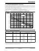
FIGURE 17-7: CLKOUT AND I/O TIMING - PIC16C5X, PIC16CR5X
TABLE 17-2: CLKOUT AND I/O TIMING REQUIREMENTS - PIC16C5X, PIC16CR5X
AC Characteristics
Standard Operating Conditions (unless otherwise specified)
Operating Temperature 0°C T
A +70C for commercial
–40C T
A +85C for industrial
–40C T
A +125C for extended
Param
No.
Symbol Characteristic Min Typ† Max Units
10 TosH2ckL OSC1 to CLKOUT
(1)
— 15 30** ns
11 TosH2ckH OSC1 to CLKOUT
(1)
— 15 30** ns
12 TckR CLKOUT rise time
(1)
— 5.0 15** ns
13 TckF CLKOUT fall time
(1)
— 5.0 15** ns
14 TckL2ioV CLKOUT to Port out valid
(1)
— — 40** ns
15 TioV2ckH Port in valid before CLKOUT
(1)
0.25 TCY+30* — — ns
16 TckH2ioI Port in hold after CLKOUT
(1)
0* — — ns
17 TosH2ioV OSC1 (Q1 cycle) to Port out valid
(2)
— — 100* ns
18 TosH2ioI OSC1 (Q2 cycle) to Port input invalid
(I/O in hold time)
TBD — — ns
19 TioV2osH Port input valid to OSC1
(I/O in setup time)
TBD — — ns
20 TioR Port output rise time
(2)
— 10 25** ns
21 TioF Port output fall time
(2)
— 10 25** ns
* These parameters are characterized but not tested.
** These parameters are design targets and are not tested. No characterization data available at this time.
† Data in the Typical (“Typ”) column is at 5V, 25°C unless otherwise stated. These parameters are for design
guidance only and are not tested.
Note 1: Measurements are taken in RC Mode where CLKOUT output is 4 x T
OSC.
2: Refer to Figure 17-5 for load conditions
.
OSC1
CLKOUT
I/O Pin
(input)
I/O Pin
(output)
Q4
Q1
Q2 Q3
10
13
14
17
20, 21
18
15
11
12
16
Old Value
New Value
19
Note: Refer to Figure 17-5 for load conditions.