
Datasheet


PIC16C5X
DS30453E-page 140 Preliminary 1997-2013 Microchip Technology Inc.
17.5 Timing Diagrams and Specifications
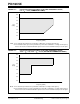
FIGURE 17-6: EXTERNAL CLOCK TIMING - PIC16C5X, PIC16CR5X
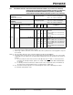
TABLE 17-1: EXTERNAL CLOCK TIMING REQUIREMENTS - PIC16C5X, PIC16CR5X
AC Characteristics
Standard Operating Conditions (unless otherwise specified)
Operating Temperature 0C T
A +70C for commercial
–40C T
A +85C for industrial
–40C T
A +125C for extended
Param
No.
Symbol Characteristic Min Typ† Max Units Conditions
F
OSC External CLKIN Frequency
(1)
DC — 4.0 MHz XT OSC mode
DC — 4.0 MHz HS
OSC mode (04)
DC — 20 MHz HS
OSC mode (20)
DC — 200 kHz LP
OSC mode
Oscillator Frequency
(1)
DC — 4.0 MHz RC OSC mode
0.45 — 4.0 MHz XT
OSC mode
4.0 — 4.0 MHz HS
OSC mode (04)
4.0 — 20 MHz HS
OSC mode (20)
5.0 — 200 kHz LP
OSC mode
1T
OSC External CLKIN Period
(1)
250 — — ns XT OSC mode
250 — — ns HS
OSC mode (04)
50 — — ns HS
OSC mode (20)
5.0 — — sLP
OSC mode
Oscillator Period
(1)
250 — — ns RC OSC mode
250 — 2,200 ns XT
OSC mode
250 — 250 ns HS
OSC mode (04)
50 — 250 ns HS
OSC mode (20)
5.0 — 200 sLP
OSC mode
* These parameters are characterized but not tested.
† Data in the Typical (“Typ”) column is at 5V, 25°C unless otherwise stated. These parameters are for design
guidance only and are not tested.
Note 1: All specified values are based on characterization data for that particular oscillator type under standard oper-
ating conditions with the device executing code. Exceeding these specified limits may result in an unstable
oscillator operation and/or higher than expected current consumption.
When an external clock input is used, the “max” cycle time limit is “DC” (no clock) for all devices.
2: Instruction cycle period (T
CY) equals four times the input oscillator time base period.
OSC1
CLKOUT
Q4
Q1 Q2
Q3 Q4 Q1
133
44
2