
Datasheet


PIC16C5X
DS30453E-page 110 Preliminary 1997-2013 Microchip Technology Inc.
15.5 Timing Parameter Symbology and Load Conditions
The timing parameter symbols have been created with one of the following formats:
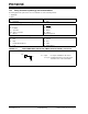
FIGURE 15-1: LOAD CONDITIONS FOR DEVICE TIMING SPECIFICATIONS - PIC16C54A
1. TppS2ppS
2. TppS
T
F Frequency T Time
Lowercase letters (pp) and their meanings:
pp
2to mcMCLR
ck CLKOUT osc oscillator
cy cycle time os OSC1
drt device reset timer t0 T0CKI
io I/O port wdt watchdog timer
Uppercase letters and their meanings:
S
FFall PPeriod
HHigh RRise
I Invalid (Hi-impedance) V Valid
L Low Z Hi-impedance
CL = 50 pF for all pins and OSC2 for RC modes
0 -15 pF for OSC2 in XT, HS or LP modes when
external clock is used to drive OSC1
CL
VSS
Pin