
Information


PIC16C505
DS80060D-page 4 © 2007 Microchip Technology Inc.
Clarifications/Corrections to the Data
Sheet:
In the Device Data Sheet (DS40192C), the following
clarifications and corrections should be noted.
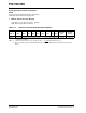
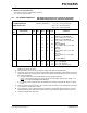
1. Module: Special Function Register
Corrections to the Special Function Register
(SFR) Summary are shown in Table 4-1.
TABLE 4-1: SPECIAL FUNCTION REGISTER (SFR) SUMMARY
Address Name Bit 7 Bit 6 Bit 5 Bit 4 Bit 3 Bit 2 Bit 1 Bit 0
Value on
Power-On
Reset
Value on
All Other
Resets
(2)
04h
FSR
Indirect Data Memory Address Pointer
100x xxxx 10uu uuuu
Legend: Shaded cells not used by PORT Registers, read as ‘0’, – = unimplemented, read as ‘0’, x = unknown, u = unchanged,
q = depends on condition.
Note 1: If Reset was due to wake-up on pin change, then bit 7 = 1. All other Resets will cause bit 7 = 0.
2: Other (non-power-up) Resets include external Reset through MCLR
, Watchdog Timer and wake-up on pin change
Reset.