
Datasheet


PIC12(L)F1571/2
DS40001723D-page 280 2013-2015 Microchip Technology Inc.
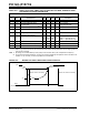
TABLE 26-14: ADC CONVERSION REQUIREMENTS
Standard Operating Conditions (unless otherwise stated)
Param.
No.
Sym. Characteristic Min. Typ† Max. Units Conditions
AD130* TAD ADC Clock Period (TADC)1.0—6.0sFOSC-based
ADC Internal FRC Oscillator Period (T
FRC)1.0 2.0 6.0s ADCS<2:0> = x11 (ADC FRC mode)
AD131 T
CNV Conversion Time
(not including Acquisition Time)
(1)
—11—TAD Set GO/DONE bit to conversion
complete
AD132* T
ACQ Acquisition Time — 5.0 — s
AD133* T
HCD Holding Capacitor Disconnect Time —
—
1/2 TAD
1/2 TAD + 1TCY
—
—
FOSC-based,
ADCS<2:0> = x11 (ADC FRC mode)
* These parameters are characterized but not tested.
† Data in “Typ” column is at 3.0V, +25°C unless otherwise stated. These parameters are for design guidance only and are
not tested.
Note 1: The ADRES register may be read on the following TCY cycle.