
Datasheet


PIC12(L)F1571/2
DS40001723D-page 278 2013-2015 Microchip Technology Inc.
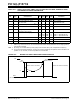
TABLE 26-13: ANALOG-TO-DIGITAL CONVERTER (ADC) CHARACTERISTICS
(1,2,3)
Operating Conditions (unless otherwise stated)
VDD = 3.0V, TA = +25°C
Param.
No.
Sym. Characteristic Min. Typ† Max. Units Conditions
AD01 NR Resolution — — 10 bit
AD02 E
IL Integral Error — ±1 ±1.7 LSb VREF = 3.0V
AD03 E
DL Differential Error — ±1 ±1 LSb No missing codes, VREF = 3.0V
AD04 E
OFF Offset Error — ±1 ±2.5 LSb VREF = 3.0V
AD05 E
GN Gain Error — ±1 ±2.0 LSb VREF = 3.0V
AD06 V
REF Reference Voltage 1.8 — VDD VVREF = (VRPOS – VRNEG) (Note 4)
AD07 VAIN Full-Scale Range VSS —VREF V
AD08 Z
AIN Recommended Impedance of
Analog Voltage Source
—— 10k Can go higher if external 0.01 F capacitor is
present on input pin.
* These parameters are characterized but not tested.
† Data in “Typ” column is at 3.0V, +25°C unless otherwise stated. These parameters are for design guidance only and are
not tested.
Note 1: Total absolute error includes integral, differential, offset and gain errors.
2: The ADC conversion result never decreases with an increase in the input voltage and has no missing codes.
3: See Section 27.0 “DC and AC Characteristics Graphs and Charts” for operating characterization.
4: ADC VREF is selected by the ADPREF<0> bit.