
Datasheet


PIC12(L)F1571/2
DS40001723D-page 276 2013-2015 Microchip Technology Inc.
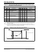
TABLE 26-11: RESET, WATCHDOG TIMER, OSCILLATOR START-UP TIMER, POWER-UP TIMER
AND BROWN-OUT RESET PARAMETERS
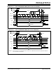
FIGURE 26-9: BROWN-OUT RESET TIMING AND CHARACTERISTICS
Standard Operating Conditions (unless otherwise stated)
Param.
No.
Sym. Characteristic Min. Typ† Max. Units Conditions
30 T
MCLMCLR Pulse Width (low) 2 — — s
31 T
WDTLP Low-Power Watchdog Timer
Time-out Period
10 16 27 ms VDD = 3.3V-5V,
1:512 prescaler used
32 T
OST Oscillator Start-up Timer Period
(1)
— 1024 — TOSC
33* TPWRT Power-up Timer Period 40 65 140 ms PWRTE = 0
34* T
IOZ I/O High-Impedance from MCLR Low
or Watchdog Timer Reset
——2.0s
35 V
BOR Brown-out Reset Voltage
(2)
2.55
2.35
1.80
2.70
2.45
1.90
2.85
2.58
2.05
V
V
V
BORV = 0
BORV = 1 (PIC12F1571/2)
BORV = 1 (PIC12LF1571/2)
36* V
HYST Brown-out Reset Hysteresis 0 25 60 mV -40°C TA +85°C
37* T
BORDC Brown-out Reset DC Response Time 1 16 35 sVDD VBOR
38 VLPBOR Low-Power Brown-out Reset Voltage 1.8 2.1 2.5 V LPBOR = 1
* These parameters are characterized but not tested.
† Data in “Typ” column is at 3.0V, +25°C unless otherwise stated. These parameters are for design guidance
only and are not tested.
Note 1: By design, the Oscillator Start-up Timer (OST) counts the first 1024 cycles, independent of frequency.
2: To ensure these voltage tolerances, V
DD and VSS must be capacitively decoupled as close to the device as
possible. 0.1 F and 0.01 F values in parallel are recommended.
VBOR
VDD
(Device in Brown-out Reset) (Device not in Brown-out Reset)
33
Reset
(due to BOR)
V
BOR and VHYST
37