
Datasheet


2013-2015 Microchip Technology Inc. DS40001723D-page 273
PIC12(L)F1571/2
TABLE 26-8: OSCILLATOR PARAMETERS
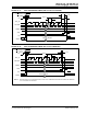
FIGURE 26-6: HFINTOSC FREQUENCY ACCURACY OVER DEVICE V
DD AND TEMPERATURE
TABLE 26-9: PLL CLOCK TIMING SPECIFICATIONS (V
DD = 2.7V TO 5.5V)
Standard Operating Conditions (unless otherwise stated)
Param.
No.
Sym. Characteristic
Freq.
Tolerance
Min. Typ† Max. Units Conditions
OS08 HFOSC Internal Calibrated HFINTOSC
Frequency
(1)
±2% — 16.0 — MHz VDD = 3.0V, TA = 25°C
(Note 2)
OS09 LFOSC Internal LFINTOSC Frequency — — 31 — kHz
OS10* T
WARM HFINTOSC
Wake-up from Sleep Start-up Time
——515s
LFINTOSC
Wake-up from Sleep Start-up Time
——0.5—ms
* These parameters are characterized but not tested.
† Data in “Typ” column is at 3.0V, +25°C unless otherwise stated. These parameters are for design guidance only and are
not tested.
Note 1: To ensure these oscillator frequency tolerances, VDD and VSS must be capacitively decoupled as close to the device as
possible. 0.1
F and 0.01 F values in parallel are recommended.
2: See Figure 26-6: “HFINTOSC Frequency Accuracy Over Device VDD and Temperature.
Param
No.
Sym. Characteristic Min. Typ† Max. Units Conditions
F10 F
OSC Oscillator Frequency Range 4 — 8 MHz
F11 F
SYS On-Chip VCO System Frequency 16 — 32 MHz
F12 TRC PLL Start-up Time (Lock Time) — — 2 ms
F13*
CLK CLKOUT Stability (Jitter) -0.25% — +0.25% %
* These parameters are characterized but not tested.
† Data in “Typ” column is at 3V, +25C unless otherwise stated. These parameters are for design guidance
only and are not tested.
+125
+25
2.0
0
+60
+85
V
DD (V)
4.0 5.04.5
Temperature (°C)
2.5
3.0
3.5 5.51.8
-40
± 5%
± 2%
± 5%
± 3%