
Datasheet


PIC12(L)F1571/2
DS40001723D-page 272 2013-2015 Microchip Technology Inc.
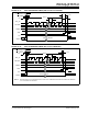
FIGURE 26-5: CLOCK TIMING
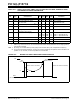
TABLE 26-7: CLOCK OSCILLATOR TIMING REQUIREMENTS
Standard Operating Conditions (unless otherwise stated)
Param.
No.
Sym. Characteristic Min. Typ† Max. Units Conditions
OS01 FOSC External CLKIN Frequency
(1)
DC — 0.5 MHz External Clock (ECL)
DC — 4 MHz External Clock (ECM)
DC — 20 MHz External Clock (ECH)
OS02 T
OSC External CLKIN Period
(1)
50 — ns External Clock (EC)
OS03 T
CY Instruction Cycle Time
(1)
200 TCY DC ns TCY = 4/FOSC
* These parameters are characterized but not tested.
† Data in “Typ” column is at 3.0V, +25°C unless otherwise stated. These parameters are for design guidance only and are
not tested.
Note 1: Instruction cycle period (TCY) equals four times the input oscillator time base period. All specified values are based on
characterization data for that particular oscillator type under standard operating conditions with the device executing code.
Exceeding these specified limits may result in an unstable oscillator operation and/or higher than expected current con-
sumption. All devices are tested to operate at “min” values with an external clock applied to the CLKIN pin. When an
external clock input is used, the “max” cycle time limit is “DC” (no clock) for all devices.
CLKIN
CLKOUT
Q4 Q1 Q2 Q3 Q4 Q1
OS02
OS03
OS04 OS04
(CLKOUT Mode)
Note 1: See Table 26-10.