
Datasheet


PIC12(L)F1571/2
DS40001723D-page 268 2013-2015 Microchip Technology Inc.
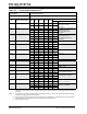
TABLE 26-4: I/O PORTS
Standard Operating Conditions (unless otherwise stated)
Param.
No.
Sym. Characteristic Min. Typ† Max. Units Conditions
VIL Input Low Voltage
I/O Ports:
D030 with TTL Buffer — — 0.8 V 4.5V
VDD 5.5V
D030A — — 0.15 V
DD V1.8V VDD 4.5V
D031 with Schmitt Trigger Buffer — — 0.2 V
DD V2.0V VDD 5.5V
with I
2
C Levels — — 0.3 VDD V
with SMbus Levels — — 0.8 V 2.7V
VDD 5.5V
D032 MCLR
——0.2VDD V
V
IH Input High Voltage
I/O Ports:
D040 with TTL Buffer 2.0 — — V 4.5V
VDD 5.5V
D040A 0.25 V
DD + 0.8 — — V 1.8V VDD 4.5V
D041 with Schmitt Trigger Buffer 0.8 V
DD ——V2.0V VDD 5.5V
with I
2
C Levels 0.7 VDD ——V
with SMbus Levels 2.1 — — V 2.7V
VDD 5.5V
D042 MCLR
0.8 VDD ——V
I
IL Input Leakage Current
(1)
D060 I/O Ports — ± 5 ± 125 nA VSS VPIN VDD,
Pin at high-impedance, +85°C
— ± 5 ± 1000 nA V
SS VPIN VDD,
Pin at high-impedance, +125°C
D061 MCLR
(2)
— ± 50 ± 200 nA VSS VPIN VDD,
Pin at high-impedance, +85°C
I
PUR Weak Pull-up Current
D070* 25 100 200 AVDD = 3.3V, VPIN = VSS
25 140 300 AVDD = 5.0V, VPIN = VSS
VOL Output Low Voltage
D080 I/O Ports — — 0.6 V IOL = 8 mA, VDD = 5V
I
OL = 6 mA, VDD = 3.3V
I
OL = 1.8 mA, VDD = 1.8V
V
OH Output High Voltage
D090 I/O Ports VDD – 0.7 — — V IOH = 3.5 mA, VDD = 5V
I
OH = 3 mA, VDD = 3.3V
I
OH = 1 mA, VDD = 1.8V
Capacitive Loading Specifications on Output Pins
D101A* CIO All I/O Pins — — 50 pF
* These parameters are characterized but not tested.
† Data in “Typ” column is at 3.0V, +25°C unless otherwise stated. These parameters are for design guidance only and are
not tested.
Note 1: Negative current is defined as current sourced by the pin.
2: The leakage current on the MCLR pin is strongly dependent on the applied voltage level. The specified levels represent
normal operating conditions. Higher leakage current may be measured at different input voltages.