
Datasheet


PIC12(L)F1571/2
DS40001723D-page 264 2013-2015 Microchip Technology Inc.
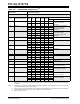
TABLE 26-2: SUPPLY CURRENT (IDD)
(1,2)
PIC12LF1571/2 Standard Operating Conditions (unless otherwise stated)
PIC12F1571/2
Param.
No.
Device
Characteristics
Min. Typ† Max. Units
Conditions
V
DD Note
D013 — 35 44 A1.8FOSC = 1 MHz,
External Clock (ECM),
Medium Power mode
—6069A3.0
D013 — 68 93 A 2.3 FOSC = 1 MHz,
External Clock (ECM),
Medium Power mode
— 91 120 A 3.0
— 131 160 A 5.0
D014 — 116 132 A1.8F
OSC = 4 MHz,
External Clock (ECM),
Medium Power mode
— 203 233 A3.0
D014 — 174 221 A 2.3 FOSC = 4 MHz,
External Clock (ECM),
Medium Power mode
— 234 286 A 3.0
— 299 374 A 5.0
D015 — 5.5 11 A1.8F
OSC = 31 kHz,
LFINTOSC,
-40°C T
A +85°C
—7.3 12 A3.0
D015 — 13 21 A 2.3 FOSC = 31 kHz,
LFINTOSC,
-40°C T
A +85°C
— 15 24 A 3.0
— 17 25 A 5.0
D016 — 111 151 A1.8F
OSC = 500 kHz,
MFINTOSC
— 133 176 A3.0
D016 — 144 209 A 2.3 FOSC = 500 kHz,
MFINTOSC
— 162 237 A 3.0
— 216 288 A 5.0
D017* — 0.5 0.6 mA 1.8 FOSC = 8 MHz,
HFINTOSC
— 0.7 0.9 mA 3.0
D017* — 0.6 0.8 mA 2.3 FOSC = 8 MHz,
HFINTOSC
— 0.8 0.9 mA 3.0
— 0.9 1.0 mA 5.0
D018 — 0.7 0.8 mA 1.8 F
OSC = 16 MHz,
HFINTOSC
— 1.1 1.2 mA 3.0
D018 — 0.9 1.1 mA 2.3 FOSC = 16 MHz,
HFINTOSC
— 1.1 1.3 mA 3.0
— 1.3 1.5 mA 5.0
* These parameters are characterized but not tested.
† Data in “Typ” column is at 3.0V, +25°C unless otherwise stated. These parameters are for design guidance
only and are not tested.
Note 1: The test conditions for all I
DD measurements in active operation mode are: CLKIN = external square wave,
from rail-to-rail; all I/O pins tri-stated, pulled to V
SS; MCLR = VDD; WDT disabled.
2: The supply current is mainly a function of the operating voltage and frequency. Other factors, such as I/O
pin loading and switching rate, oscillator type, internal code execution pattern and temperature, also have
an impact on the current consumption.
3: PLL required for 32 MHz operation.