
Datasheet


PIC12(L)F1571/2
DS40001723D-page 262 2013-2015 Microchip Technology Inc.
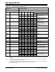
26.3 DC Characteristics
TABLE 26-1: SUPPLY VOLTAGE
PIC12LF1571/2 Standard Operating Conditions (unless otherwise stated)
PIC12F1571/2
Param.
No.
Sym. Characteristic Min. Typ† Max. Units Conditions
D001 VDD Supply Voltage
VDDMIN
1.8
2.5
—
—
V
DDMAX
3.6
3.6
V
V
FOSC 16 MHz
F
OSC 32 MHz (Note 3)
D001 2.3
2.5
—
—
5.5
5.5
V
V
FOSC 16 MHz
F
OSC 32 MHz (Note 3)
D002* VDR RAM Data Retention Voltage
(1)
1.5 — — V Device in Sleep mode
D002* 1.7 — — V Device in Sleep mode
D002A* V
POR Power-on Reset Release Voltage
(2)
—1.6— V
D002A* — 1.6 — V
D002B* VPORR* Power-on Reset Rearm Voltage
(2)
—0.8— V
D002B* — 1.5 — V
D003 VFVR Fixed Voltage Reference Voltage — 1.024 — V -40°C TA +85°C
D003A V
ADFVR FVR Gain Voltage Accuracy for
ADC
-4 — +4 %
1x V
FVR, ADFVR = 01, VDD 2.5V
2x V
FVR, ADFVR = 10, VDD 2.5V
4x V
FVR, ADFVR = 11, VDD 4.75V
D003B V
CDAFVR FVR Gain Voltage Accuracy for
Comparator
-4 — +4 %
1x V
FVR, CDAFVR = 01, VDD 2.5V
2x V
FVR, CDAFVR = 10, VDD 2.5V
4x V
FVR, CDAFVR = 11, VDD 4.75V
D004* SV
DD VDD Rise Rate
(2)
0.05 — — V/ms Ensures that the Power-on Reset
signal is released properly
* These parameters are characterized but not tested.
† Data in “Typ” column is at 3.0V, +25°C unless otherwise stated. These parameters are for design guidance only and are
not tested.
Note 1: This is the limit to which VDD can be lowered in Sleep mode without losing RAM data.
2: See Figure 26-3, POR and POR Rearm with Slow Rising VDD.
3: PLL required for 32 MHz operation.