
Datasheet


2013-2015 Microchip Technology Inc. DS40001723D-page 239
PIC12(L)F1571/2
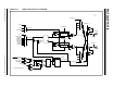
REGISTER 23-2: CWGxCON1: CWGx CONTROL REGISTER 1
R/W-x/u R/W-x/u R/W-x/u R/W-x/u U-0 R/W-0/0 R/W-0/0 R/W-0/0
GxASDLB<1:0> GxASDLA<1:0> — GxIS<2:0>
bit 7 bit 0
Legend:
R = Readable bit W = Writable bit
u = Bit is unchanged x = Bit is unknown U = Unimplemented bit, read as ‘0’
‘1’ = Bit is set ‘0’ = Bit is cleared -n/n = Value at POR and BOR/Value at all other Resets
bit 7-6 GxASDLB<1:0>: CWGx Shutdown State for CWGxB bits
When an Auto-Shutdown Event is Present (GxASE =
1):
11 = CWGxB pin is driven to ‘1’, regardless of the setting of the GxPOLB bit
10 = CWGxB pin is driven to ‘0’, regardless of the setting of the GxPOLB bit
01 = CWGxB pin is tri-stated
00 = CWGxB pin is driven to its inactive state after the selected dead-band interval; GxPOLB will still
control the polarity of the output
bit 5-4 GxASDLA<1:0>: CWGx Shutdown State for CWGxA bits
When an Auto-Shutdown Event is Present (GxASE =
1):
11 = CWGxA pin is driven to ‘1’, regardless of the setting of the GxPOLA bit
10 = CWGxA pin is driven to ‘0’, regardless of the setting of the GxPOLA bit
01 = CWGxA pin is tri-stated
00 = CWGxA pin is driven to its inactive state after the selected dead-band interval; GxPOLA will still
control the polarity of the output
bit 3 Unimplemented: Read as ‘0’
bit 2-0 GxIS<2:0>: CWGx Input Source Select bits
111 =Reserved
110 =Reserved
101 =Reserved
100 = PWM3 – PWM3_out
011 = PWM2 – PWM2_out
010 = PWM1 – PWM1_out
001 =Reserved
000 = Comparator C1 – C1OUT_async