
Datasheet


PIC12(L)F1571/2
DS40001723D-page 238 2013-2015 Microchip Technology Inc.
23.12 Register Definitions: CWG Control
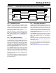
REGISTER 23-1: CWGxCON0: CWGx CONTROL REGISTER 0
R/W-0/0 R/W-0/0 R/W-0/0 R/W-0/0 R/W-0/0 U-0 U-0 R/W-0/0
GxEN GxOEB GxOEA GxPOLB GxPOLA
— —GxCS0
bit 7 bit 0
Legend:
R = Readable bit W = Writable bit
u = Bit is unchanged x = Bit is unknown U = Unimplemented bit, read as ‘0’
‘1’ = Bit is set ‘0’ = Bit is cleared -n/n = Value at POR and BOR/Value at all other Resets
bit 7 GxEN: CWGx Enable bit
1 = Module is enabled
0 = Module is disabled
bit 6 GxOEB: CWGxB Output Enable bit
1 = CWGxB is available on appropriate I/O pin
0 = CWGxB is not available on appropriate I/O pin
bit 5 GxOEA: CWGxA Output Enable bit
1 = CWGxA is available on appropriate I/O pin
0 = CWGxA is not available on appropriate I/O pin
bit 4 GxPOLB: CWGxB Output Polarity bit
1 = Output is inverted polarity
0 = Output is normal polarity
bit 3 GxPOLA: CWGxA Output Polarity bit
1 = Output is inverted polarity
0 = Output is normal polarity
bit 2-1 Unimplemented: Read as ‘0’
bit 0 GxCS0: CWGx Clock Source Select bit
1 =HFINTOSC
0 =F
OSC