
Datasheet


PIC12(L)F1571/2
DS40001723D-page 236 2013-2015 Microchip Technology Inc.
23.10 Operation During Sleep
The CWG module operates independently from the
system clock, and will continue to run during Sleep
provided that the clock and input sources selected
remain active.
The HFINTOSC remains active during Sleep, provided
that the CWG module is enabled, the input source is
active and the HFINTOSC is selected as the clock
source, regardless of the system clock source
selected.
In other words, if the HFINTOSC is simultaneously
selected as the system clock and the CWG clock
source, when the CWG is enabled and the input source
is active, the CPU will go idle during Sleep, but the
CWG will continue to operate and the HFINTOSC will
remain active.
This will have a direct effect on the Sleep mode current.
23.11 Configuring the CWG
The following steps illustrate how to properly configure
the CWG to ensure a synchronous start:
1. Ensure that the TRISx control bits correspond-
ing to CWGxA and CWGxB are set so that both
are configured as inputs.
2. Clear the GxEN bit if not already cleared.
3. Set desired dead-band times with the CWGxDBR
and CWGxDBF registers.
4. Set up the following controls in the CWGxCON2
auto-shutdown register:
• Select desired shutdown source.
• Select both output overrides to the desired
levels (this is necessary even if not using
auto-shutdown because start-up will be from
a shutdown state).
• Set the GxASE bit and clear the GxARSEN
bit.
5. Select the desired input source using the
CWGxCON1 register.
6. Configure the following controls in the
CWGxCON0 register:
• Select desired clock source.
• Select the desired output polarities.
• Set the output enables for the outputs to be
used.
7. Set the GxEN bit.
8. Clear the TRISx control bits corresponding to
CWGxA and CWGxB to be used to configure
those pins as outputs.
9. If auto-restart is to be used, set the GxARSEN
bit and the GxASE bit will be cleared automati-
cally. Otherwise, clear the GxASE bit to start the
CWG.
23.11.1 PIN OVERRIDE LEVELS
The levels driven to the output pins, while the shutdown
input is true, are controlled by the GxASDLA
and GxASDLB bits of the CWGxCON1 register
(Register 23-3). GxASDLA controls the CWG1A over-
ride level and GxASDLB controls the CWG1B override
level. The control bit logic level corresponds to the out-
put logic drive level while in the shutdown state. The
polarity control does not apply to the override level.
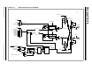
23.11.2 AUTO-SHUTDOWN RESTART
After an auto-shutdown event has occurred, there are
two ways to resume operation:
• Software controlled
• Auto-restart
The restart method is selected with the GxARSEN bit
of the CWGxCON2 register. Waveforms of software
controlled and automatic restarts are shown in
Figure 23-5 and Figure 23-6.
23.11.2.1 Software Controlled Restart
When the GxARSEN bit of the CWGxCON2 register
is cleared, the CWG must be restarted after an
auto-shutdown event by software.
Clearing the shutdown state requires all selected shut-
down inputs to be low, otherwise, the GxASE bit will
remain set. The overrides will remain in effect until the
first rising edge event after the GxASE bit is cleared.
The CWG will then resume operation.
23.11.2.2 Auto-Restart
When the GxARSEN bit of the CWGxCON2 register is
set, the CWG will restart from the auto-shutdown state
automatically.
The GxASE bit will clear automatically when all shut-
down sources go low. The overrides will remain in
effect until the first rising edge event after the GxASE
bit is cleared. The CWG will then resume operation.