
Datasheet


2013-2015 Microchip Technology Inc. DS40001723D-page 219
PIC12(L)F1571/2
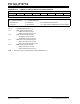
REGISTER 22-4: PWMxCLKCON: PWMx CLOCK CONTROL REGISTER
U-0 R/W-0/0 R/W-0/0 R/W-0/0 U-0 U-0 R/W-0/0 R/W-0/0
—PS<2:0>— — CS<1:0>
bit 7 bit 0
Legend:
R = Readable bit W = Writable bit
u = Bit is unchanged x = Bit is unknown U = Unimplemented bit, read as ‘0’
‘1’ = Bit is set ‘0’ = Bit is cleared -n/n = Value at POR and BOR/Value at all other Resets
bit 7 Unimplemented: Read as ‘0’
bit 6-4 PS<2:0>: Clock Source Prescaler Select bits
111 = Divides clock source by 128
110 = Divides clock source by 64
101 = Divides clock source by 32
100 = Divides clock source by 16
011 = Divides clock source by 8
010 = Divides clock source by 4
001 = Divides clock source by 2
000 = No prescaler
bit 3-2 Unimplemented: Read as ‘0’
bit 1-0 CS<1:0>: Clock Source Select bits
11 = Reserved
10 = LFINTOSC (continues to operate during Sleep)
01 = HFINTOSC (continues to operate during Sleep)
00 =FOSC