
Datasheet


2013-2015 Microchip Technology Inc. DS40001723D-page 217
PIC12(L)F1571/2
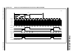
REGISTER 22-2: PWMxINTE: PWMx INTERRUPT ENABLE REGISTER
U-0 U-0 U-0 U-0 R/W-0/0 R/W-0/0 R/W-0/0 R/W-0/0
— — — — OFIE PHIE DCIE PRIE
bit 7 bit 0
Legend:
R = Readable bit W = Writable bit
u = Bit is unchanged x = Bit is unknown U = Unimplemented bit, read as ‘0’
‘1’ = Bit is set ‘0’ = Bit is cleared -n/n = Value at POR and BOR/Value at all other Resets
bit 7-4 Unimplemented: Read as ‘0’
bit 3 OFIE: Offset Interrupt Enable bit
1 = Interrupts CPU on offset match
0 = Does not interrupt CPU on offset match
bit 2 PHIE: Phase Interrupt Enable bit
1 = Interrupts CPU on phase match
0 = Does not Interrupt CPU on phase match
bit 1 DCIE: Duty Cycle Interrupt Enable bit
1 = Interrupts CPU on duty cycle match
0 = Does not interrupt CPU on duty cycle match
bit 0 PRIE: Period Interrupt Enable bit
1 = Interrupts CPU on period match
0 = Does not interrupt CPU on period match