
Datasheet


PIC12(L)F1571/2
DS40001723D-page 216 2013-2015 Microchip Technology Inc.
22.7 Register Definitions: PWM Control
Long bit name prefixes for the 16-bit PWM peripherals
are shown in Table 22-1. Refer to Section
1.1 “Register and Bit Naming Conventions” for more
information
TABLE 22-1: BIT NAME PREFIXES
Peripheral Bit Name Prefix
PWM1 PWM1
PWM2 PWM2
PWM3 PWM3
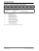
REGISTER 22-1: PWMxCON: PWMx CONTROL REGISTER
R/W-0/0 R/W-0/0 R/HS/HC-0/0 R/W-0/0 R/W-0/0 R/W-0/0 U-0 U-0
EN OE OUT POL MODE<1:0> — —
bit 7 bit 0
Legend:
HC = Hardware Clearable bit HS = Hardware Settable bit
R = Readable bit W = Writable bit U = Unimplemented bit, read as ‘0’
‘1’ = Bit is set ‘0’ = Bit is cleared -n/n = Value at POR and BOR/Value at all other Resets
bit 7 EN: PWMx Module Enable bit
1 = Module is enabled
0 = Module is disabled
bit 6 OE: PWMx Output Enable bit
1 = PWM output pin is enabled
0 = PWM output pin is disabled
bit 5 OUT: Output State of the PWMx Module bit
bit 4 POL: PWMx Output Polarity Control bit
1 = PWM output active state is low
0 = PWM output active state is high
bit 3-2 MODE<1:0>: PWMx Mode Control bits
11 = Center-Aligned mode
10 = Toggle On Match mode
01 = Set On Match mode
00 = Standard PWM mode
bit 1-0 Unimplemented: Read as ‘0’