
Datasheet


2013-2015 Microchip Technology Inc. DS40001723D-page 215
PIC12(L)F1571/2
22.4 Reload Operation
Four of the PWM module control register pairs and one
control bit are double-buffered so that all can be
updated simultaneously. These include:
• PWMxPHH:PWMxPHL register pair
• PWMxDCH:PWMxDCL register pair
• PWMxPRH:PWMxPRL register pair
• PWMxOFH:PWMxOFL register pair
• OFO control bit
When written to, these registers do not immediately
affect the operation of the PWM. By default, writes to
these registers will not be loaded into the PWM Oper-
ating Buffer registers until after the arming conditions
are met. The arming control has two methods of
operation:
• Immediate
• Triggered
The LDT bit of the PWMxLDCON register controls the
arming method. Both methods require the LDA bit to be
set. All four buffer pairs will load simultaneously at the
loading event.
22.4.1 IMMEDIATE RELOAD
When the LDT bit is clear, then the immediate mode is
selected and the buffers will be loaded at the first period
event after the LDA bit is set. Immediate reloading is
used when a PWM module is operating stand-alone or
when the PWM module is operating as a master to
other slave PWM modules.
22.4.2 TRIGGERED RELOAD
When the LDT bit is set, then the Triggered mode is
selected and a trigger event is required for the LDA bit
to take effect. The trigger source is the buffer load
event of one of the other PWM modules in the device.
The triggering source is selected by the LDS<1:0> bits
of the PWMxLDCON register. The buffers will be
loaded at the first period event following the trigger
event. Triggered reloading is used when a PWM
module is operating as a slave to another PWM and it
is necessary to synchronize the buffer reloads in both
modules.
22.5 Operation in Sleep Mode
Each PWM module will continue to operate in Sleep
mode when either the HFINTOSC or LFINTOSC is
selected as the clock source by PWMxCLKCON<1:0>.
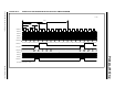
22.6 Interrupts
Each PWM module has four independent interrupts
based on the phase, duty cycle, period and offset match
events. The interrupt flag is set on the rising edge of
each of these signals. Refer to Figures 22-12 and 22-13
for detailed timing diagrams of the match signals.
Note 1: The buffer load operation clears the
LDA bit.
2: If the LDA bit is set at the same time as
PWMxTMR = PWMxPR, the LDA bit is
ignored until the next period event. Such
is the case when triggered reload is
selected and the triggering event occurs
simultaneously with the target’s period
event.