
Datasheet


PIC12(L)F1571/2
DS40001723D-page 204 2013-2015 Microchip Technology Inc.
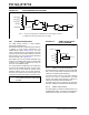
FIGURE 22-2: LOAD TRIGGER BLOCK DIAGRAM
22.1 Fundamental Operation
The PWM module produces a 16-bit resolution
pulse-width modulated output.
Each PWM module has an independent timer driven by
a selection of clock sources determined by the
PWMxCLKCON register (Register 22-4). The timer
value is compared to event count registers to generate
the various events of a the PWM waveform, such as the
period and duty cycle. For a block diagram describing
the clock sources, refer to Figure 22-3.
Each PWM module can be enabled individually using
the EN bit of the PWMxCON register, or several PWM
modules can be enabled simultaneously using the
mirror bits of the PWMEN register.
The current state of the PWM output can be read using
the OUT bit of the PWMxCON register. In some modes,
this bit can be set and cleared by software, giving
additional software control over the PWM waveform.
This bit is synchronized to F
OSC/4 and therefore, does
not change in real time with respect to the PWM_clock.
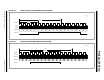
FIGURE 22-3: PWM CLOCK SOURCE
BLOCK DIAGRAM
22.1.1 PWMx PIN CONFIGURATION
All PWM outputs are multiplexed with the PORT data
latch, so the pins must also be configured as outputs by
clearing the associated PORT TRISx bits.
The slew rate feature may be configured to optimize
the rate to be used in conjunction with the PWM
outputs. High-speed output switching is attained by
clearing the associated PORT SLRCONx bits.
The PWM outputs can be configured to be open-drain
outputs by setting the associated PORT ODCONx bits.
22.1.2 PWMx Output Polarity
The output polarity is inverted by setting the POL bit of
the PWMxCON register. The polarity control affects the
PWM output even when the module is not enabled.
Rev. 10-000153A
4/21/2014
00
11
10
01
LD3_trigger
(1)
LD2_trigger
(1)
LD1_trigger
(1)
Reserved
PWMxLDS PRx_match
1
0
PWMxLDA
(2)
DQ
PWM_clock
LDx_trigger
PWMxLDT
Note 1. The input corresponding to a PWM module’s own load trigger is reserved.
2. PWMxLDA is cleared by hardware upon LDx_trigger.
Note: If PWM_clock > FOSC/4, the OUT bit may
not accurately represent the output state of
the PWM.
Rev. 10-000156A
1/7/2015
00
11
10
01
HFINTOSC
LFINTOSC
F
OSC
Reserved
PWMxCS<1:0>
Prescaler PWMx_clock
PWMxPS<2:0>