
Datasheet


2013-2015 Microchip Technology Inc. DS40001723D-page 201
PIC12(L)F1571/2
21.5.2.3 EUSART Synchronous Slave
Reception
The operation of the Synchronous Master and Slave
modes is identical (Section 21.5.1.5 “Synchronous
Master Reception”), with the following exceptions:
• Sleep
• CREN bit is always set, therefore, the receiver is
never Idle
• SREN bit, which is a “don’t care” in Slave mode
A character may be received while in Sleep mode by
setting the CREN bit prior to entering Sleep. Once the
word is received, the RSR register will transfer the data
to the RCREG register. If the RCIE enable bit is set, the
interrupt generated will wake the device from Sleep
and execute the next instruction. If the GIE bit is also
set, the program will branch to the interrupt vector.
21.5.2.4 Synchronous Slave Reception Setup
1. Set the SYNC and SPEN bits, and clear the
CSRC bit.
2. Clear the ANSELx bit for both the CK and DT
pins (if applicable).
3. If interrupts are desired, set the RCIE bit of the
PIE1 register, and the GIE and PEIE bits of the
INTCON register.
4. If 9-bit reception is desired, set the RX9 bit.
5. Set the CREN bit to enable reception.
6. The RCIF bit will be set when reception is
complete. An interrupt will be generated if the
RCIE bit was set.
7. If 9-bit mode is enabled, retrieve the Most
Significant bit from the RX9D bit of the RCSTA
register.
8. Retrieve the eight Least Significant bits from the
receive FIFO by reading the RCREG register.
9. If an overrun error occurs, clear the error by
either clearing the CREN bit of the RCSTA
register or by clearing the SPEN bit which resets
the EUSART.
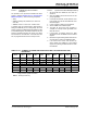
TABLE 21-10: SUMMARY OF REGISTERS ASSOCIATED WITH SYNCHRONOUS SLAVE
RECEPTION
Name Bit 7 Bit 6 Bit 5 Bit 4 Bit 3 Bit 2 Bit 1 Bit 0
Register
on Page
BAUDCON
ABDOVF RCIDL —SCKPBRG16 — WUE ABDEN 186
INTCON GIE PEIE TMR0IE INTE IOCIE TMR0IF INTF IOCIF 74
PIE1
TMR1GIE ADIE RCIE
(1)
TXIE
(1)
— — TMR2IE TMR1IE 75
PIR1 TMR1GIF ADIF RCIF
(1)
TXIF
(1)
— — TMR2IF TMR1IF 78
RCREG EUSART Receive Data Register 180*
RCSTA SPEN RX9 SREN CREN ADDEN FERR OERR RX9D 185
TXSTA CSRC TX9 TXEN SYNC
SENDB BRGH TRMT TX9D 184
Legend: — = unimplemented location, read as ‘0’. Shaded cells are not used for synchronous slave reception.
* Page provides register information.
Note 1: PIC12(L)F1572 only.