
Datasheet


PIC12(L)F1571/2
DS40001723D-page 180 2013-2015 Microchip Technology Inc.
21.1.2 EUSART ASYNCHRONOUS
RECEIVER
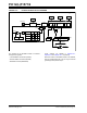
The Asynchronous mode is typically used in RS-232
systems. The receiver block diagram is shown in
Figure 21-2. The data is received on the RX/DT pin and
drives the data recovery block. The data recovery block
is actually a high-speed shifter operating at 16 times
the baud rate, whereas the serial Receive Shift
Register (RSR) operates at the bit rate. When all eight
or nine bits of the character have been shifted in, they
are immediately transferred to a two character
First-In-First-Out (FIFO) memory. The FIFO buffering
allows reception of two complete characters and the
start of a third character before software must start ser-
vicing the EUSART receiver. The FIFO and RSR regis-
ters are not directly accessible by software. Access to
the received data is via the RCREG register.
21.1.2.1 Enabling the Receiver
The EUSART receiver is enabled for asynchronous
operation by configuring the following three control bits:
• CREN = 1
• SYNC = 0
• SPEN = 1
All other EUSART control bits are assumed to be in
their default state.
Setting the CREN bit of the RCSTA register enables the
receiver circuitry of the EUSART. Clearing the SYNC bit
of the TXSTA register configures the EUSART for asyn-
chronous operation. Setting the SPEN bit of the RCSTA
register enables the EUSART. The programmer must
set the corresponding TRIS bit to configure the RX/DT
I/O pin as an input.
21.1.2.2 Receiving Data
The receiver data recovery circuit initiates character
reception on the falling edge of the first bit. The first bit,
also known as the Start bit, is always a zero. The data
recovery circuit counts one-half bit time to the center of
the Start bit and verifies that the bit is still a zero. If it is
not a zero then the data recovery circuit aborts charac-
ter reception, without generating an error, and resumes
looking for the falling edge of the Start bit. If the Start bit
zero verification succeeds, then the data recovery
circuit counts a full bit time to the center of the next bit.
The bit is then sampled by a majority detect circuit and
the resulting ‘0’ or ‘1’ is shifted into the RSR. This
repeats until all data bits have been sampled and
shifted into the RSR. One final bit time is measured and
the level sampled. This is the Stop bit, which is always
a ‘1’. If the data recovery circuit samples a ‘0’ in the
Stop bit position then a framing error is set for this char-
acter; otherwise, the framing error is cleared for this
character. See Section 21.1.2.4 “Receive Framing
Error” for more information on framing errors.
Immediately after all data bits and the Stop bit have
been received, the character in the RSR is transferred
to the EUSART receive FIFO and the RCIF interrupt
flag bit of the PIR1 register is set. The top character in
the FIFO is transferred out of the FIFO by reading the
RCREG register.
21.1.2.3 Receive Interrupts
The RCIF interrupt flag bit of the PIR1 register is set
whenever the EUSART receiver is enabled and there is
an unread character in the receive FIFO. The RCIF
interrupt flag bit is read-only, it cannot be set or cleared
by software.
RCIF interrupts are enabled by setting all of the
following bits:
• RCIE, Interrupt Enable bit of the PIE1 register
• PEIE, Peripheral Interrupt Enable bit of the
INTCON register
• GIE, Global Interrupt Enable bit of the INTCON
register
The RCIF interrupt flag bit will be set when there is an
unread character in the FIFO, regardless of the state of
interrupt enable bits.
Note: If the RX/DT function is on an analog pin,
the corresponding ANSELx bit must be
cleared for the receiver to function.
Note: If the receive FIFO is overrun, no
additional characters will be received
until the overrun condition is cleared. See
Section 21.1.2.5 “Receive Overrun
Error” for more information on overrun
errors.