
Datasheet


2013-2015 Microchip Technology Inc. DS40001723D-page 169
PIC12(L)F1571/2
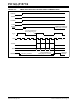
TABLE 19-5: SUMMARY OF REGISTERS ASSOCIATED WITH TIMER1
Name Bit 7 Bit 6 Bit 5 Bit 4 Bit 3 Bit 2 Bit 1 Bit 0
Register
on Page
ANSELA
— — — ANSA4 — ANSA<2:0> 114
APFCON RXDTSEL CWGASEL CWGBSEL — T1GSEL TXCKSEL P2SEL P1SEL 110
INTCON GIE PEIE
TMR0IE INTE IOCIE TMR0IF INTF IOCIF 74
OSCSTAT —PLLROSTS HFIOFR HFIOFL MFIOFR LFIOFR HFIOFS 56
PIE1 TMR1GIE ADIE RCIE
(2)
TXIE
(2)
— — TMR2IE TMR1IE 75
PIR1 TMR1GIF ADIF RCIF
(2)
TXIF
(2)
— — TMR2IF TMR1IF 79
TMR1H Holding Register for the Most Significant Byte of the 16-bit TMR1 Count 163*
TMR1L Holding Register for the Least Significant Byte of the 16-bit TMR1 Count 163*
TRISA
— — TRISA<5:4> —
(1)
TRISA<2:0> 113
T1CON TMR1CS<1:0> T1CKPS<1:0>
— T1SYNC —TMR1ON167
T1GCON TMR1GE T1GPOL T1GTM T1GSPM T1GGO/
DONE
T1GVAL T1GSS<1:0> 168
Legend: — = unimplemented location, read as ‘0’. Shaded cells are not used by the Timer1 module.
* Page provides register information.
Note 1: Unimplemented, read as ‘1’.
2: PIC12(L)F1572 only.