
Datasheet


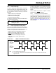


2013-2015 Microchip Technology Inc. DS40001723D-page 167
PIC12(L)F1571/2
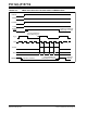
19.8 Register Definitions: Timer1 Control
REGISTER 19-1: T1CON: TIMER1 CONTROL REGISTER
R/W-0/u R/W-0/u R/W-0/u R/W-0/u U-0 R/W-0/u U-0 R/W-0/u
TMR1CS<1:0> T1CKPS<1:0>
— T1SYNC —TMR1ON
bit 7 bit 0
Legend:
R = Readable bit W = Writable bit
u = Bit is unchanged x = Bit is unknown U = Unimplemented bit, read as ‘0’
‘1’ = Bit is set ‘0’ = Bit is cleared -n/n = Value at POR and BOR/Value at all other Resets
bit 7-6 TMR1CS<1:0>: Timer1 Clock Source Select bits
11 = Timer1 clock source is the LFINTOSC
10 = Timer1 clock source is the T1CKI pin (on the rising edge)
01 = Timer1 clock source is the system clock (F
OSC)
00 = Timer1 clock source is the instruction clock (F
OSC/4)
bit 5-4 T1CKPS<1:0>: Timer1 Input Clock Prescale Select bits
11 = 1:8 Prescale value
10 = 1:4 Prescale value
01 = 1:2 Prescale value
00 = 1:1 Prescale value
bit 3 Unimplemented: Read as ‘0’
bit 2 T
1SYNC: Timer1 Synchronization Control bit
1 = Does not synchronize the asynchronous clock input
0 = Synchronizes the asynchronous clock input with the system clock (F
OSC)
bit 1 Unimplemented: Read as ‘0’
bit 0 TMR1ON: Timer1 On bit
1 = Enables Timer1
0 = Stops Timer1 and clears Timer1 gate flip-flop