
Datasheet


2013-2015 Microchip Technology Inc. DS40001723D-page 145
PIC12(L)F1571/2
16.6 Register Definitions: DAC Control
TABLE 16-1: SUMMARY OF REGISTERS ASSOCIATED WITH THE DAC MODULE
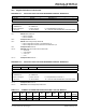
REGISTER 16-1: DACxCON0: DACx VOLTAGE REFERENCE CONTROL REGISTER 0
R/W-0/0 U-0 R/W-0/0 U-0 R/W-0/0 R/W-0/0 U-0 U-0
DACEN —DACOE— DACPSS<1:0> — —
bit 7 bit 0
Legend:
R = Readable bit W = Writable bit
u = Bit is unchanged x = Bit is unknown U = Unimplemented bit, read as ‘0’
‘1’ = Bit is set ‘0’ = Bit is cleared -n/n = Value at POR and BOR/Value at all other Resets
bit 7 DACEN: DAC Enable bit
1 = DACx is enabled
0 = DACx is disabled
bit 6 Unimplemented: Read as ‘0’
bit 5 DACOE: DAC Voltage Output Enable bit
1 = DACx voltage level is output on the DACxOUT1 pin
0 = DACx voltage level is disconnected from the DACxOUT1 pin
bit 4 Unimplemented: Read as ‘0’
bit 3-2 DACPSS<1:0>: DAC Positive Source Select bits
11 = Reserved
10 = FVR_buffer2
01 =V
REF+ pin
00 =V
DD
bit 1-0 Unimplemented: Read as ‘0’
REGISTER 16-2: DACxCON1: DACx VOLTAGE REFERENCE CONTROL REGISTER 1
U-0 U-0 U-0 R/W-0/0 R/W-0/0 R/W-0/0 R/W-0/0 R/W-0/0
— — — DACR<4:0>
bit 7 bit 0
Legend:
R = Readable bit W = Writable bit
u = Bit is unchanged x = Bit is unknown U = Unimplemented bit, read as ‘0’
‘1’ = Bit is set ‘0’ = Bit is cleared -n/n = Value at POR and BOR/Value at all other Resets
bit 7-5 Unimplemented: Read as ‘0’
bit 4-0 DACR<4:0>: DAC Voltage Output Select bits
Name Bit 7 Bit 6 Bit 5 Bit 4 Bit 3 Bit 2 Bit 1 Bit 0
Register
on Page
DACxCON0 DACEN
—DACOE— DACPSS<1:0> — — 145
DACxCON1 — — — DACR<4:0> 145
Legend: — = Unimplemented location, read as ‘0’.