
Datasheet


2013-2015 Microchip Technology Inc. DS40001723D-page 137
PIC12(L)F1571/2
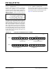
REGISTER 15-3: ADCON2: ADC CONTROL REGISTER 2
R/W-0/0 R/W-0/0 R/W-0/0 R/W-0/0 U-0 U-0 U-0 U-0
TRIGSEL<3:0>
(1)
— — — —
bit 7 bit 0
Legend:
R = Readable bit W = Writable bit
u = Bit is unchanged x = Bit is unknown U = Unimplemented bit, read as ‘0’
‘1’ = Bit is set ‘0’ = Bit is cleared -n/n = Value at POR and BOR/Value at all other Resets
bit 7-4 TRIGSEL<3:0>: Auto-Conversion Trigger Selection bits
(1)
0000 = No auto-conversion trigger selected
0001 = PWM1 – PWM1_interrupt
0010 = PWM2 – PWM2_interrupt
0011 = Timer0 – T0_overflow
(2)
0100 = Timer1 – T1_overflow
(2)
0101 = Timer2 – T2_match
0110 = Comparator C1 – C1OUT_sync
0111 = PWM3 – PWM3_interrupt
1000 = PWM1 – PWM1_OF1_match
1001 = PWM2 – PWM2_OF2_match
1010 = PWM3 – PWM3_OF3_match
1011 = Reserved
1100 = Reserved
1101 = Reserved
1110 = Reserved
1111 = Reserved
bit 3-0 Unimplemented: Read as ‘0’
Note 1: This is a rising edge sensitive input for all sources.
2: Signal also sets its corresponding interrupt flag.