
Datasheet


2013-2015 Microchip Technology Inc. DS40001723D-page 133
PIC12(L)F1571/2
15.2 ADC Operation
15.2.1 STARTING A CONVERSION
To enable the ADC module, the ADON bit of the
ADCON0 register must be set to a ‘1’. Setting the
GO/DONE bit of the ADCON0 register to a ‘1’ will start
the Analog-to-Digital conversion.
15.2.2 COMPLETION OF A CONVERSION
When the conversion is complete, the ADC module will:
• Clear the GO/DONE
bit
• Set the ADIF Interrupt Flag bit
• Update the ADRESH and ADRESL registers with
new conversion result
15.2.3 TERMINATING A CONVERSION
If a conversion must be terminated before completion,
the GO/DONE
bit can be cleared in software. The
ADRESH and ADRESL registers will be updated with
the partially complete Analog-to-Digital conversion
sample. Incomplete bits will match the last bit
converted.
15.2.4 ADC OPERATION DURING SLEEP
The ADC module can operate during Sleep. This
requires the ADC clock source to be set to the FRC
option. Performing the ADC conversion during Sleep
can reduce system noise. If the ADC interrupt is
enabled, the device will wake-up from Sleep when the
conversion completes. If the ADC interrupt is disabled,
the ADC module is turned off after the conversion
completes, although the ADON bit remains set.
When the ADC clock source is something other than
FRC, a SLEEP instruction causes the present conver-
sion to be aborted and the ADC module is turned off,
although the ADON bit remains set.
15.2.5 AUTO-CONVERSION TRIGGER
The auto-conversion trigger allows periodic ADC
measurements without software intervention. When a
rising edge of the selected source occurs, the
GO/DONE
bit is set by hardware.
The auto-conversion trigger source is selected with the
TRIGSEL<3:0> bits of the ADCON2 register.
Using the auto-conversion trigger does not assure
proper ADC timing. It is the user’s responsibility to
ensure that the ADC timing requirements are met.
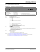
The PWM module can trigger the ADC in two ways,
directly through the PWMx_OFx_match or through the
interrupts generated by all four match signals. See
Section 22.0 “16-Bit Pulse-Width Modulation (PWM)
Module”. If the interrupts are chosen, each enabled
interrupt in PWMxINTE will trigger a conversion. Refer
to Figure 15-4 for more information.
See Table 15-2 for auto-conversion sources.
FIGURE 15-4: 16-BIT PWM INTERRUPT
BLOCK DIAGRAM
Note: The GO/DONE bit should not be set in the
same instruction that turns on the ADC.
Refer to Section 15.2.6 “ADC Conversion
Procedure”.
Note: A device Reset forces all registers to their
Reset state. Thus, the ADC module is
turned off and any pending conversion is
terminated.
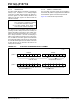
TABLE 15-2: AUTO-CONVERSION
SOURCES
Source Peripheral Signal Name
Timer0 T0_overflow
Timer1 T1_overflow
Timer2 T2_match
Comparator C1 C1OUT_sync
PWM1 PWM1_OF_match
PWM1 PWM1_interrupt
PWM2 PWM2_OF_match
PWM2 PWM2_interrupt
PWM3 PWM3_OF_match
PWM3 PWM3_interrupt
Rev. 10-000154A
10/24/2013
PWMx_interrupt
PWMxOFIE
PWMxPHIE
PWMxDCIE
PWMxPRIE
OFx_match
PRx_match
DCx_match
PHx_match