
Datasheet


PIC12(L)F1571/2
DS40001723D-page 110 2013-2015 Microchip Technology Inc.
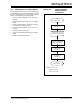
11.1 Alternate Pin Function
The Alternate Pin Function Control (APFCON) register
is used to steer specific peripheral input and output
functions between different pins. The APFCON register
is shown in Register 11-1. For this device family, the
following functions can be moved between different
pins.
•RX/DT
•TX/CK
• CWGOUTA
• CWGOUTB
•PWM2
•PWM1
These bits have no effect on the values of any TRISx
register. PORTx and TRISx overrides will be routed to
the correct pin. The unselected pin will be unaffected.
11.2 Register Definitions: Alternate Pin Function Control
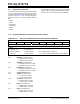
REGISTER 11-1: APFCON: ALTERNATE PIN FUNCTION CONTROL REGISTER
R/W-0/0 R/W-0/0 R/W-0/0 U-0 R/W-0/0 R/W-0/0 R/W-0/0 R/W-0/0
RXDTSEL CWGASEL CWGBSEL — T1GSEL TXCKSEL P2SEL P1SEL
bit 7 bit 0
Legend:
R = Readable bit W = Writable bit
u = Bit is unchanged x = Bit is unknown U = Unimplemented bit, read as ‘0’
‘1’ = Bit is set ‘0’ = Bit is cleared -n/n = Value at POR and BOR/Value at all other Resets
bit 7 RXDTSEL: Pin Selection bit
1 = RX/DT function is on RA5
0 = RX/DT function is on RA1
bit 6 CWGASEL: Pin Selection bit
1 = CWGOUTA function is on RA5
0 = CWGOUTA function is on RA2
bit 5 CWGBSEL: Pin Selection bit
1 = CWGOUTB function is on RA4
0 = CWGOUTB function is on RA0
bit 4 Unimplemented: Read as ‘0’
bit 3 T1GSEL: Pin Selection bit
1 = T1G function is on RA3
0 = T1G function is on RA4
bit 2 TXCKSEL: Pin Selection bit
1 = TX/CK function is on RA4
0 = TX/CK function is on RA0
bit 1 P2SEL: Pin Selection bit
1 = PWM2 function is on RA4
0 = PWM2 function is on RA0
bit 0 P1SEL: Pin Selection bit
1 = PWM1 function is on RA5
0 = PWM1 function is on RA1