
Datasheet


2013-2015 Microchip Technology Inc. DS40001723D-page 107
PIC12(L)F1571/2
TABLE 10-3: SUMMARY OF REGISTERS ASSOCIATED WITH FLASH PROGRAM MEMORY
TABLE 10-4: SUMMARY OF CONFIGURATION WORD WITH FLASH PROGRAM MEMORY
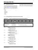
REGISTER 10-6: PMCON2: PROGRAM MEMORY CONTROL 2 REGISTER
W-0/0 W-0/0 W-0/0 W-0/0 W-0/0 W-0/0 W-0/0 W-0/0
Program Memory Control Register 2
bit 7 bit 0
Legend:
R = Readable bit W = Writable bit
S = Bit can only be set x = Bit is unknown U = Unimplemented bit, read as ‘0’
‘1’ = Bit is set ‘0’ = Bit is cleared -n/n = Value at POR and BOR/Value at all other Resets
bit 7-0 Flash Memory Unlock Pattern bits
To unlock writes, a 55h must be written first, followed by an AAh, before setting the WR bit of the
PMCON1 register. The value written to this register is used to unlock the writes. There are specific
timing requirements on these writes.
Name Bit 7 Bit 6 Bit 5 Bit 4 Bit 3 Bit 2 Bit 1 Bit 0
Register
on Page
INTCON GIE PEIE TMR0IE INTE IOCIE TMR0IF INTF IOCIF 74
PMCON1 —
(1)
CFGS LWLO FREE WRERR WREN WR RD 106
PMCON2 Program Memory Control Register 2 107
PMADRL PMADRL<7:0> 105
PMADRH
—
(1)
PMADRH<6:0> 105
PMDATL PMDATL<7:0> 104
PMDATH
— —PMDATH<5:0>104
Legend: — = unimplemented location, read as ‘0’. Shaded cells are not used by Flash program memory.
Note 1: Unimplemented, read as ‘1’.
Name Bits Bit -/7 Bit -/6 Bit 13/5 Bit 12/4 Bit 11/3 Bit 10/2 Bit 9/1 Bit 8/0
Register
on Page
CONFIG1
13:8
— — — — CLKOUTEN BOREN<1:0> —
42
7:0 CP
MCLRE PWRTE WDTE<1:0> — FOSC<1:0>
CONFIG2
13:8
— — LVP DEBUG LPBOR BORV STVREN PLLEN
43
7:0 — — — — — —WRT<1:0>
Legend: — = unimplemented location, read as ‘0’. Shaded cells are not used by Flash program memory.