
Information
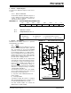


PIC12C67X
DS80067C-page 8 2001 Microchip Technology Inc.
6. Module: DC Characteristics
Corrections for the DC Characteristics, Sections 12.3
and 12.4 are shown.
12.3 DC CHARACTERISTICS: PIC12C671/672 (Commercial, Industrial, Extended)
PIC12CE673/674 (Commercial, Industrial, Extended)
12.4 DC CHARACTERISTICS: PIC12LC671/672 (Commercial, Industrial)
PIC12LCE673/674 (Commercial, Industrial)
DC CHARACTERISTICS
Standard Operating Conditions (unless otherwise specified)
Operating temperature 0°C ≤ TA ≤ +70°C (commercial)
–40°C ≤ T
A ≤ +85°C (industrial)
–40°C ≤ T
A ≤ +125°C (extended)
Operating voltage V
DD range as described in DC spec Section 12.1 and
Section 12.2.
Param
No.
Characteristic Sym Min Typ† Max Units Conditions
Input Leakage Current (Notes 2, 3)
I
IL
D061 GP3/MCLR (Note 5)
8 130
250 µAVSS ≤ VPIN ≤ VDD
D061A GP3/MCLR (Note 6) +5 µAVSS ≤ VPIN ≤ VDD
D070 GPIO weak pull-up current (Note 4) IPUR 50 250 400 µAVDD = 5V, VPIN = VSS
† Data in “Typ” column is at 5V, 25
°
C unless otherwise stated. These parameters are for design guidance only and are not
tested.
Note 1:
In EXTRC oscillator configuration, the OSC1/CLKIN pin is a Schmitt Trigger input. It is not recommended that the
PIC12C67X
be driven with external clock in RC mode.
2: The leakage current on the MCLR
pin is strongly dependent on the applied voltage level. The specified levels represent
normal operating conditions. Higher leakage current may be measured at different input voltages.
3: Negative current is defined as coming out of the pin.
4: Does not include GP3. For GP3 see parameters D061 and D061A.
5: This spec. applies to GP3/MCLR
configured as external MCLR and GP3/MCLR configured as input with internal pull-up
enabled.
6: This spec. applies when GP3/MCLR
is configured as an input with pull-up disabled. The leakage current of the MCLR circuit
is higher than the standard I/O logic.
DC CHARACTERISTICS
Standard Operating Conditions (unless otherwise specified)
Operating temperature 0°C ≤ T
A ≤ +70°C (commercial)
–40°C ≤ T
A ≤ +85°C (industrial)
Operating voltage V
DD range as described in DC spec Section 12.1 and
Section 12.2.
Param
No.
Characteristic Sym Min Typ† Max Units Conditions
Input Leakage Current (Notes 2, 3)
I
IL
D061 GP3/MCLR (Note 5)
8130
250 µAVss ≤ VPIN ≤ VDD
D061A GP3/MCLR (Note 6) +5 µAVss ≤ VPIN ≤ VDD
D070 GPIO weak pull-up current (Note 4) IPUR 50 250 400 µAVDD = 5V, VPIN = VSS
† Data in “Typ” column is at 5V, 25
°
C unless otherwise stated. These parameters are for design guidance only and are not
tested.
Note 1:
In EXTRC oscillator configuration, the OSC1/CLKIN pin is a Schmitt Trigger input. It is not recommended that the
PIC12C67X
be driven with external clock in RC mode.
2: The leakage current on the MCLR
pin is strongly dependent on the applied voltage level. The specified levels represent nor-
mal operating conditions. Higher leakage current may be measured at different input voltages.
3: Negative current is defined as coming out of the pin.
4: Does not include GP3. For GP3 see parameters D061 and D061A.
5: This spec. applies to GP3/MCLR
configured as external MCLR and GP3/MCLR configured as input with internal pull-up
enabled.
6: This spec. applies when GP3/MCLR
is configured as an input with pull-up disabled. The leakage current of the MCLR circuit is
higher than the standard I/O logic.