PIC12C67X PIC12C67X Rev. A Silicon/Data Sheet Errata The PIC12C67X (Rev. A) parts you have received conform functionally to the Device Data Sheet (DS30561), except for the anomalies described below. FIGURE 1: PIC12C67X VOLTAGE-FREQUENCY GRAPH, -40°C ≤ TA ≤ +125°C 6.0 5.5 5.0 VDD (Volts) 4.5 4.0 3.5 3.0 2.5 2.0 0 4 10 20 25 Frequency (MHz) Note 1: The shaded region indicates the permissible combinations of voltage and frequency.
PIC12C67X PIC12LC67X VOLTAGE-FREQUENCY GRAPH, -40°C ≤ TA ≤ 0°C FIGURE 2: 6.0 5.5 5.0 VDD (Volts) 4.5 4.0 3.5 3.0 2.7 2.5 2.0 0 4 10 20 25 Frequency (MHz) Note 1: The shaded region indicates the permissible combinations of voltage and frequency. 2: The maximum rated speed of the part limits the permissible combinations of voltage and frequency. Please reference the Product Identification System section for the maximum rated speed of the parts.
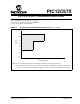
PIC12C67X FIGURE 4: PIC12LC67X VOLTAGE-FREQUENCY GRAPH, +70°C ≤ TA ≤ +85°C 6.0 5.5 5.0 VDD (Volts) 4.5 4.0 3.5 3.0 2.5 2.0 0 4 10 20 25 Frequency (MHz) Note 1: The shaded region indicates the permissible combinations of voltage and frequency. 2: The maximum rated speed of the part limits the permissible combinations of voltage and frequency. Please reference the Product Identification System section for the maximum rated speed of the parts. 2001 Microchip Technology Inc.
PIC12C67X Clarifications/Corrections to the Data Sheet: In the Device Data Sheet (DS30561B), the following clarifications and corrections should be noted. 1. Module: Register Summary (OSCCAL) In Section 4.0, corrections for the Special Function Register Summary, Table 4-1, are shown.
PIC12C67X 2. Module: OSCCAL Register Correction for the “OSCCAL” Register, Section 4.2.2.7, is shown. 4.2.2.7 OSCCAL REGISTER The Oscillator Calibration (OSCCAL) Register is used to calibrate the internal 4 MHz oscillator. It contains six bits for calibration. Increasing the value increases the frequency.
PIC12C67X FIGURE 5-2: GP2 Block Diagram FIGURE 5-4: Data bus VDD Q CK CLKOUT Enable Data bus Q D I/O Pin D WR TRIS Oscillator Circuit To OSC1 D WR PORT GP4 Block Diagram Q CK Q WR PORT Q CK VDD Fosc/4 Q 1 0 VSS Analog Input Mode RD TRIS Q D WR TRIS CK Q VSS INTRC/ EXTRC RD TRIS D I/O Pin Q Analog Input Mode EN Q RD PORT D EN TMR0 Clock Input RD PORT GP2/INT To A/D Converter FIGURE 5-3: To A/D Converter GP3 Block Diagram FIGURE 5-5: GP5 Block Diagram Data bus VDD
PIC12C67X 4. Module: OSCCAL (Oscillator) Corrections for the Internal 4 MHz RC Oscillator, Section 9.2.5, are shown. 9.2.5 INTERNAL 4 MHz RC OSCILLATOR OSCCAL, when written to with the calibration value, will “trim” the internal oscillator to remove process variation from the oscillator frequency. Only bits<7:2> of OSCCAL are implemented, and bits<1:0> should be written as 0 for compatibility with future devices. The oscillator calibration location is not code protected. 5.
PIC12C67X 6. Module: DC Characteristics Corrections for the DC Characteristics, Sections 12.3 and 12.4 are shown. 12.3 DC CHARACTERISTICS: DC CHARACTERISTICS Param No.
PIC12C67X 7. Module: GPIO Register Corrections for the GPIO pull-up resistor ranges are shown in Table 12-6. TABLE 12-6: VDD (Volts) GPIO PULL-UP RESISTOR RANGES Temperature (°C) Min Typ Max Units GP0/GP1 2.5 5.
PIC12C67X 8. Module: PACKAGING INFORMATION Added 8-Lead Plastic Micro Leadframe Package (MF) and (MLF-S). 8-Lead Plastic Micro Leadframe Package (MF) 6x5 mm Body (MLF-S) E p B E1 n L R D1 1 D D2 PIN 1 ID EXPOSED METAL PADS 2 E2 TOP VIEW BOTTOM VIEW α A2 A3 A A1 INCHES Units Dimension Limits Number of Pins MIN MILLIMETERS* NOM n MAX MIN NOM 8 MAX 8 Pitch p Overall Height A .033 .039 0.85 1.00 Molded Package Thickness A2 .026 .031 0.65 0.80 Standoff A1 .0004 .
PIC12C67X 8-Lead Plastic Micro Leadframe Package (MF) 6x5 mm Body (MLF-S) M SOLDER MASK M p B PACKAGE EDGE L Units Pitch Dimension Limits p INCHES MIN NOM MILLIMETERS* MAX MIN .050 BSC NOM MAX 1.27 BSC Pad Width B .014 .016 .019 0.35 0.40 0.47 Pad Length L .020 .024 .030 0.50 0.60 0.75 Pad to Solder Mask M .005 .006 0.13 0.15 *Controlling Parameter Drawing No. C04-2113 2001 Microchip Technology Inc.
PIC12C67X REVISION HISTORY Rev A Document (2/01) Original errata document, which includes Figures 1, 2, and 3. Rev B Document (6/00) Under the Clarifications/Corrections, Items 1 through 7 were added. Rev C Document (11/01) Added Figure 1 and renumbered figures accordingly. Under the Clarifications/Corrections, added Figures 5-1 through 5-5 added to Item 3. Item 8, added 8-Lead Plastic Micro Leadframe Package (MF/MLF-S). DS80067C-page 12 2001 Microchip Technology Inc.
Note the following details of the code protection feature on PICmicro® MCUs. • • • • • • The PICmicro family meets the specifications contained in the Microchip Data Sheet. Microchip believes that its family of PICmicro microcontrollers is one of the most secure products of its kind on the market today, when used in the intended manner and under normal conditions. There are dishonest and possibly illegal methods used to breach the code protection feature.
WORLDWIDE SALES AND SERVICE AMERICAS ASIA/PACIFIC Japan Corporate Office Australia 2355 West Chandler Blvd. Chandler, AZ 85224-6199 Tel: 480-792-7200 Fax: 480-792-7277 Technical Support: 480-792-7627 Web Address: http://www.microchip.com Microchip Technology Australia Pty Ltd Suite 22, 41 Rawson Street Epping 2121, NSW Australia Tel: 61-2-9868-6733 Fax: 61-2-9868-6755 Microchip Technology Japan K.K.