
Information


PIC12C508A/C509A/CR509A
2003 Microchip Technology Inc. DS80063D-page 3
Clarifications/Corrections to the Data Sheet:
In the Device Data Sheet (DS40139E), the following
clarifications and corrections should be noted.
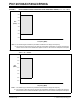
1. Valid regions of operation:
FIGURE 4: PIC12C508A/C509A/CR509A VOLTAGE FREQUENCY GRAPH, -40°C ≤ TA ≤ +125°C
2. Section 13: Corrections for the DC Characteristics,
Sections 13.1, 13.2, 13.3, and 13.4 are shown.
Corrections for the GPIO pull-up resistor ranges
are shown in Table 13-1. For the section titled
“RESET”, additional information is provided on
OSC1/CLKIN and OSC2/CLKOUT pin states
during a MCLR
.
6.0
2.5
4.0
3.0
0
3.5
4.5
5.0
5.5
410
Frequency (MHz)
V
DD
20
(Volts)
25
Note 1: The shaded region indicates the permissible combinations of voltage and frequency.
2: The maximum rated speed of the part limits the permissible combinations of voltage and frequency.
Please reference the Product Identification System section for the maximum rated speed of the parts.