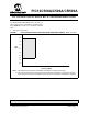
PIC12C508A/C509A/CR509A PIC12C508A/C509A/CR509A Rev. B Silicon/Data Sheet Errata The PIC12C508A/C509A/CR509A (Rev. B) parts you have received conform functionally to the Device Data Sheet (DS40139), except for the anomalies described below. 1. Valid regions of operation: FIGURE 1: PIC12LC508A/LC509A/LCR509A VOLTAGE FREQUENCY GRAPH, -40°C ≤ TA ≤ 0°C 6.0 5.5 5.0 4.5 VDD (Volts) 4.0 3.5 3.0 2.7 2.5 2.
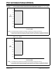
PIC12C508A/C509A/CR509A PIC12LC508A/LC509A/LCR509A VOLTAGE FREQUENCY GRAPH, 0°C ≤ TA ≤ +70°C FIGURE 2: 6.0 5.5 5.0 4.5 VDD (Volts) 4.0 3.5 3.0 2.5 2.0 0 4 10 20 25 Frequency (MHz) Note 1: The shaded region indicates the permissible combinations of voltage and frequency. 2: The maximum rated speed of the part limits the permissible combinations of voltage and frequency. Please reference the Product Identification System section for the maximum rated speed of the parts.
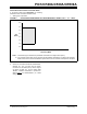
PIC12C508A/C509A/CR509A Clarifications/Corrections to the Data Sheet: In the Device Data Sheet (DS40139E), the following clarifications and corrections should be noted. 1. Valid regions of operation: FIGURE 4: PIC12C508A/C509A/CR509A VOLTAGE FREQUENCY GRAPH, -40°C ≤ TA ≤ +125°C 6.0 5.5 5.0 VDD (Volts) 4.5 4.0 3.5 3.0 2.5 0 4 10 20 25 Frequency (MHz) Note 1: The shaded region indicates the permissible combinations of voltage and frequency.
PIC12C508A/C509A/CR509A 13.1 DC CHARACTERISTICS: PIC12C508A/509A (Commercial, Industrial, Extended) PIC12CE518/519 (Commercial, Industrial, Extended) PIC12CR509A (Commercial, Industrial, Extended) Standard Operating Conditions (unless otherwise specified) Operating Temperature 0°C ≤ TA ≤ +70°C (commercial) -40°C ≤ TA ≤ +85°C (industrial) -40°C ≤ TA ≤ +125°C (extended) DC Characteristics Power Supply Pins Parm No. Characteristic Sym Min Typ(1) Max Units 5.5 V D001 Supply Voltage VDD 3.
PIC12C508A/C509A/CR509A 13.2 DC CHARACTERISTICS: PIC12LC508A/509A (Commercial, Industrial) PIC12LCE518/519 (Commercial, Industrial) PIC12LCR509A (Commercial, Industrial) Standard Operating Conditions (unless otherwise specified) Operating Temperature 0°C ≤ TA ≤ +70°C (commercial) -40°C ≤ TA ≤ +85°C (industrial) DC Characteristics Power Supply Pins Parm No. Characteristic Sym Min Typ(1) Max D001 Supply Voltage VDD 2.
PIC12C508A/C509A/CR509A 13.3 DC CHARACTERISTICS: DC CHARACTERISTICS Param No.
PIC12C508A/C509A/CR509A 13.4 DC CHARACTERISTICS: DC CHARACTERISTICS Param No.
PIC12C508A/C509A/CR509A TABLE 13-1: PULL-UP RESISTOR RANGES* - PIC12C508A, PIC12C509A, PIC12CR509A, PIC12CE518, PIC12CE519, PIC12LC508A, PIC12LC509A, PIC12LCR509A, PIC12LCE518 and PIC12LCE519 VDD (Volts) Temperature (°C) Min 2.5 -40 25 85 125 -40 25 85 125 38K 42K 42K 50K 15K 18K 19K 22K Typ Max Units 42K 48K 49K 55K 17K 20K 22K 24K 63K 63K 63K 63K 20K 23K 25K 28K Ω Ω Ω Ω Ω Ω Ω Ω GP0/GP1 5.5 GP3(1) 2.5 5.
PIC12C508A/C509A/CR509A 3. Module: Packaging The package information contained in the data sheet is incorrect. Please refer to the following tables for correct package data.
PIC12C508A/C509A/CR509A 8-Lead Plastic Small Outline (SM) – Medium, 208 mil (SOIC) E E1 p D 2 1 n B α c A2 A φ L β Units Dimension Limits n p Number of Pins Pitch Overall Height Molded Package Thickness Standoff § Overall Width Molded Package Width Overall Length Foot Length Foot Angle Lead Thickness Lead Width Mold Draft Angle Top Mold Draft Angle Bottom * Controlling Parameter § Significant Characteristic A A2 A1 E E1 D L φ c B α β MIN .070 .069 .002 .300 .201 .202 .020 0 .008 .
PIC12C508A/C509A/CR509A 8-Lead Ceramic Side Brazed Dual In-line with Window (JW) – 300 mil E1 W T D 2 1 n U A A2 L A1 c B1 eB Units Dimension Limits n p Number of Pins Pitch Top to Seating Plane Top of Body to Seating Plane Standoff Package Width Overall Length Tip to Seating Plane Lead Thickness Upper Lead Width Lower Lead Width Overall Row Spacing § Window Diameter Lid Length Lid Width * Controlling Parameter § Significant Characteristic JEDC Equivalent: MS-015 Drawing No.
PIC12C508A/C509A/CR509A 8-Lead Plastic Small Outline (SN) – Narrow, 150 mil (SOIC) E E1 p D 2 B n 1 h α 45° c A2 A φ β L Units Dimension Limits n p Number of Pins Pitch Overall Height Molded Package Thickness Standoff § Overall Width Molded Package Width Overall Length Chamfer Distance Foot Length Foot Angle Lead Thickness Lead Width Mold Draft Angle Top Mold Draft Angle Bottom * Controlling Parameter § Significant Characteristic A A2 A1 E E1 D h L φ c B α β MIN .053 .052 .004 .228 .146 .
PIC12C508A/C509A/CR509A 8-Lead Plastic Dual Flat No Lead Package (MF) 6x5 mm Body (DFN-S) E p B E1 n L R D1 1 D D2 PIN 1 ID EXPOSED METAL PADS 2 E2 TOP VIEW BOTTOM VIEW α A2 A3 A A1 Units Dimension Limits Number of Pins MILLIMETERS* INCHES MIN NOM n MAX MIN NOM MAX 8 8 Pitch p Overall Height A .033 .039 0.85 1.00 Molded Package Thickness A2 .026 .031 0.65 0.80 Standoff A1 .0004 .002 0.01 0.05 Base Thickness A3 .008 REF. 0.20 REF. 4.92 BSC Overall Length .
PIC12C508A/C509A/CR509A APPENDIX A: REVISION HISTORY Rev. D Document (6/2003) Under Clarifications/Corrections to the Data Sheet, Item 3, Packaging: correct package data was added. Added Appendix A: Revision History. DS80063D-page 14 2003 Microchip Technology Inc.
Note the following details of the code protection feature on Microchip devices: • Microchip products meet the specification contained in their particular Microchip Data Sheet. • Microchip believes that its family of products is one of the most secure families of its kind on the market today, when used in the intended manner and under normal conditions. • There are dishonest and possibly illegal methods used to breach the code protection feature.
WORLDWIDE SALES AND SERVICE AMERICAS ASIA/PACIFIC Japan Corporate Office Australia 2355 West Chandler Blvd. Chandler, AZ 85224-6199 Tel: 480-792-7200 Fax: 480-792-7277 Technical Support: 480-792-7627 Web Address: http://www.microchip.com Microchip Technology Australia Pty Ltd Marketing Support Division Suite 22, 41 Rawson Street Epping 2121, NSW Australia Tel: 61-2-9868-6733 Fax: 61-2-9868-6755 Microchip Technology Japan K.K.