
Information


DS80063D-page 8 2003 Microchip Technology Inc.
PIC12C508A/C509A/CR509A
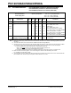
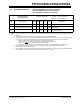
TABLE 13-1: PULL-UP RESISTOR RANGES* - PIC12C508A, PIC12C509A, PIC12CR509A,
PIC12CE518, PIC12CE519, PIC12LC508A, PIC12LC509A, PIC12LCR509A,
PIC12LCE518 and PIC12LCE519
RESET
When MCLR is asserted, the state of the OSC1/CLKIN
and CLKOUT/OSC2 pins are as follows:
V
DD (Volts) Temperature (°C) Min Typ Max Units
GP0/GP1
2.5 -40 38K 42K 63K Ω
25 42K 48K 63K Ω
85 42K 49K 63K Ω
125 50K 55K 63K Ω
5.5 -40 15K 17K 20K Ω
25 18K 20K 23K Ω
85 19K 22K 25K Ω
125 22K 24K 28K Ω
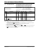
GP3
(1)
2.5 -40
65K
80K
850K
Ω
25
80K
100K
1150K
Ω
85
85K
110K
1300K
Ω
125
100K
120K
1500K
Ω
5.5 -40
50K
60K
600K
Ω
25
60K
65K
750K
Ω
85
65K
80K
900K
Ω
125
75K
90K
990K
Ω
* These parameters are characterized but not tested.
Note 1: The weak pull-up resistor and associated current for the GP3/MCLR
pin is non-linear when the respective
pin voltage is less than V
DD - 1.0V. See parameter D061 for GP3/MCLR pin current specifications.
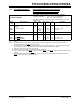
CLKIN/CLKOUT PIN STATES WHEN MCLR
ASSERTED
Oscillator Mode OSC1/CLKIN Pin OSC2/CLKOUT Pin
EXTRC, CLKOUT
on OSC2
OSC1 pin is
tristated and
driven by external
circuit
OSC2 pin is driven
low
EXTRC, OSC2 is
I/O
OSC1 pin is
tristated and
driven by external
circuit
OSC2 pin is tristate
input
INTRC, CLKOUT
on OSC2
OSC1 pin is
tristate input
OSC2 pin is driven
low
INTRC, OSC2 is
I/O
OSC1 pin is
tristate input
OSC2 pin is tristate
input