
User manual


PIC10F200/202/204/206
DS41239A-page 72 Preliminary 2004 Microchip Technology Inc.
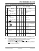
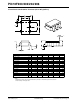
TABLE 12-4: CALIBRATED INTERNAL RC FREQUENCIES – PIC10F200/202/204/206
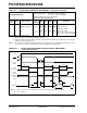
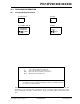
FIGURE 12-3: RESET, WATCHDOG TIMER AND DEVICE RESET TIMER TIMING –
PIC10F200/202/204/206
AC CHARACTERISTICS
Standard Operating Conditions (unless otherwise specified)
Operating Temperature -40°C ≤ T
A ≤ +85°C (industrial),
-40°C ≤ T
A ≤ +125°C (extended)
Operating Voltage V
DD range is described in
Section 12.1 “DC Characteristics”.
Param
No.
Sym Characteristic
Freq
Tolerance
Min Typ† Max Units Conditions
F10 F
OSC Internal Calibrated
INTOSC Frequency
(1)
± 1% TBD 4.00 TBD MHz VDD and Temperature TBD
± 2% TBD 4.00 TBD MHz 2.5V ≤ V
DD ≤ 5.5V
Temperature TBD
± 5% TBD 4.00 TBD MHz 2.0V ≤ V
DD ≤ 5.5V
-40°C ≤ T
A ≤ +85°C (industrial)
-40°C ≤ T
A ≤ +125°C (extended)
Legend: TBD = To Be Determined.
* These parameters are characterized but not tested.
† Data in the Typical (“Typ”) column is at 5V, 25°C unless otherwise stated. These parameters are for design
guidance only and are not tested.
Note 1: To ensure these oscillator frequency tolerances, V
DD and VSS must be capacitively decoupled as close to
the device as possible. 0.1 µF and 0.01 µF values in parallel are recommended.
VDD
MCLR
Internal
POR
DRT
Timeout
(2)
Internal
Reset
Watchdog
Timer
Reset
32
31
34
I/O pin
(1)
32
32
34
30
Note 1: I/O pins must be taken out of High-impedance mode by enabling the output drivers in software.
2: Runs on POR only.