
User's Manual

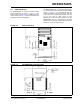
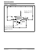

Table Of Contents
- Features
- Operational
- RF/Analog Features
- Media Access Controller (MAC)/ Baseband Features
- Pin diagram
- Table of Contents
- Most Current Data Sheet
- Errata
- Customer Notification System
- 1.0 Device Overview
- 2.0 Circuit Description
- 3.0 Regulatory Approval
- 4.0 Electrical Characteristics
- Appendix A: Revision History
- Product Identification System
- Corporate Office
- Atlanta
- Boston
- Chicago
- Cleveland
- Fax: 216-447-0643
- Dallas
- Detroit
- Indianapolis
- Toronto
- Fax: 852-2401-3431
- Australia - Sydney
- China - Beijing
- China - Shanghai
- India - Bangalore
- Korea - Daegu
- Korea - Seoul
- Singapore
- Taiwan - Taipei
- Fax: 43-7242-2244-393
- Denmark - Copenhagen
- France - Paris
- Germany - Munich
- Italy - Milan
- Spain - Madrid
- UK - Wokingham
- Worldwide Sales and Service

© 2011 Microchip Technology Inc. Preliminary DS00000A-page 7
MRF89XAM9A
1.3 Operation
The MRF89XAM9A module is based on the Microchip
Technology MRF89XA Ultra Low-Power, Integrated
ISM Band Sub-GHz Transceiver IC. Data
communication and module configuration are
documented in the “MRF89XA Ultra Low-Power,
Integrated ISM Band Sub-GHz Transceiver Data
Sheet” (DS70622).
This section emphasizes operational settings that are
unique to the MRF89XAM9A module design that must
be followed for proper operation.
1.3.1 RESET
Pin 2 of the module, RESET, allows for an external
reset of the MRF89XA IC. RESET is connected to the
TEST8 pin of the MRF89XA IC. During normal
operations of the MRF89XAM9A, the RESET pin
should be held in a high impedance state. For more
information on Assertion of the RESET pin, refer to the
“Section 3.1.2 Manual Reset” of “MRF89XA Data
Sheet” (DS70622).
1.3.2 CRYSTAL FREQUENCY
When calculating frequency deviation, bit rate, receiver
bandwidth, and PLL R, P and S values, use crystal
frequency f
xtal
= 12.8 MHz.
1.3.3 CLOCK OUTPUT (CLKOUT)
The CLKOUT pin 19 of the MRF89XA IC is not used on
the module. Ensure that the CLKOUT signal is disabled
to minimize the current consumption.
1.3.4 FREQUENCY BAND SELECT
The Frequency Band Select (FBS<1:0>) bits in the
GCONREG<4:3> should be set for target channel
range 902–915 MHz FBS<1:0> = '00' or 915–928 MHz
FBS<1:0> = '01'.
1.3.5 VCO TANK TRIM VALUE
The VCO Trim (VCOT<1:0>) bits in the
GCONREG<2:1> should be set for VCOT<1:0> = '11'
for the inductor values of the module.