
User's Manual

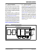
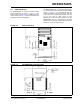

Table Of Contents
- Features
- Operational
- RF/Analog Features
- Media Access Controller (MAC)/ Baseband Features
- Pin diagram
- Table of Contents
- Most Current Data Sheet
- Errata
- Customer Notification System
- 1.0 Device Overview
- 2.0 Circuit Description
- 3.0 Regulatory Approval
- 4.0 Electrical Characteristics
- Appendix A: Revision History
- Product Identification System
- Corporate Office
- Atlanta
- Boston
- Chicago
- Cleveland
- Fax: 216-447-0643
- Dallas
- Detroit
- Indianapolis
- Toronto
- Fax: 852-2401-3431
- Australia - Sydney
- China - Beijing
- China - Shanghai
- India - Bangalore
- Korea - Daegu
- Korea - Seoul
- Singapore
- Taiwan - Taipei
- Fax: 43-7242-2244-393
- Denmark - Copenhagen
- France - Paris
- Germany - Munich
- Italy - Milan
- Spain - Madrid
- UK - Wokingham
- Worldwide Sales and Service

© 2011 Microchip Technology Inc. Preliminary DS00000A-page 3
MRF89XAM9A
1.0 DEVICE OVERVIEW
The MRF89XAM9A is an Ultra Low-Power Sub-GHz
surface mount transceiver module with integrated
crystal, internal voltage regulator, matching circuitry
and PCB antenna. The MRF89XAM9A module
operates in the United States/Canada 902–928 MHz
ISM frequency band. The integrated module design
frees the integrator from extensive RF and antenna
design, and regulatory compliance testing, allowing
quicker time to market.
The MRF89XAM9A module is compatible with
Microchip’s MiWi™ Development Environment software
stacks. The software stacks are available as a free
download, including source code, from the Microchip’s
web site http://www.microchip.com/wireless.
The MRF89XAM9A module has received regulatory
approvals for modular devices in the United States
(FCC) and Canada (IC). Modular approval removes the
need for expensive RF and antenna design, and allows
the end user to place the MRF89XAM9A module inside
a finished product and not require regulatory testing for
an intentional radiator (RF transmitter). To maintain
conformance, refer to module settings in Section 3.1.1,
MRF89XAM9A SETTINGS for the United States and
Section 3.2.1, MRF89XAM9A SETTINGS for Canada.
1.1 Interface description
The simplified block diagram of the MRF89XAM9A
module is shown in Figure 1-1. The module is based on
the Microchip Technology MRF89XA Ultra Low-Power
Sub-GHz Transceiver Integrated Circuit (IC). The
module interfaces to many popular Microchip PIC
®
microcontrollers through a 3-wire serial SPI interface,
two chip selects (Configuration and Data), two
interrupts — Interrupt Request 0 (IRQ0) and Interrupt
Request 1 (IRQ1), Reset, Power and Ground as shown
in Figure 1-2. Tab le 1-1 provides the pin descriptions.
Data communication and module configuration are
documented in the “MRF89XA Ultra Low-Power,
Integrated Sub-GHz Transceiver” (DS70622) Data
Sheet. For more information on specific serial interface
protocol and general register definitions, refer to the
“MRF89XA Data Sheet” and see Section 1.3,
Operation for specific register settings unique to the
MRF89XAM9A module operation to maintain
regulatory compliance.
FIGURE 1-1: MRF89XAM9A BLOCK DIAGRAM
MRF89XA
Control
Interface
Power
Management
BasebandRF
MRF89XAM9A Module
SPI
Digital I/O
IRQ0
Power
12.8 MHz Crystal
Matching
Circuitry
and
SAW Filter
PCB
Antenna
Loop
Filter
VCO
Tank
IRQ1
CSDATA
CSCON
RESET