
User's Manual

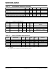
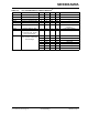
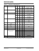
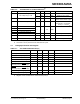

Table Of Contents
- Features
- Operational
- RF/Analog Features
- Media Access Controller (MAC)/ Baseband Features
- Pin diagram
- Table of Contents
- Most Current Data Sheet
- Errata
- Customer Notification System
- 1.0 Device Overview
- 2.0 Circuit Description
- 3.0 Regulatory Approval
- 4.0 Electrical Characteristics
- Appendix A: Revision History
- Product Identification System
- Corporate Office
- Atlanta
- Boston
- Chicago
- Cleveland
- Fax: 216-447-0643
- Dallas
- Detroit
- Indianapolis
- Toronto
- Fax: 852-2401-3431
- Australia - Sydney
- China - Beijing
- China - Shanghai
- India - Bangalore
- Korea - Daegu
- Korea - Seoul
- Singapore
- Taiwan - Taipei
- Fax: 43-7242-2244-393
- Denmark - Copenhagen
- France - Paris
- Germany - Munich
- Italy - Milan
- Spain - Madrid
- UK - Wokingham
- Worldwide Sales and Service

© 2011 Microchip Technology Inc. Preliminary DS00000A-page 25
MRF89XAM9A
TABLE 4-6: TRANSMITTER AC CHARACTERISTICS
(1)
4.1 Timing Specification and Diagram
TABLE 4-7: SPI TIMING SPECIFICATION
(1,2)
Symbol Description Min Typ Max Unit Condition
RFOP RF Output Power, Programmable
with 8 Steps of typ. 3 dB
— +12.5 — dBm Maximum power setting
— -8.5 — dBm Minimum power setting
PN Phase Noise — -112 — dBc/Hz Measured with a 600 kHz
offset at the transmitter output
TXSP Transmitted Spurious — — -47 dBc At any offset between 200 kHz
and 600 kHz, unmodulated
carrier, f
dev
= 50 kHz
Tx2 Second Harmonic
——-40dBm
No modulation, see Note
(2)
Tx3 Third Harmonic
Tx4 Fourth Harmonic
Txn Harmonics above Tx4
FSKDEV FSK Deviation ±33 ±55 ±200 kHz Programmable
TSTWF Transmitter Wake-up Time — 120 500 µs From FS to Tx ready
TSTWS Transmitter Wake-up Time — 600 900 µs From Stand-by to Tx ready
Note 1: Guaranteed by design and characterization.
2: Transmitter in-circuit performance with SAW filter and crystal.
Parameter Min Typ Max Unit Condition
SPI Configure Clock Frequency — — 6 MHz —
SPI Data Clock Frequency — — 1 MHz —
Data Hold and Setup Time 2 — — µs —
SDI Setup Time for SPI Configure 250 — — ns —
SDI Setup Time for SPI Data 312 — — ns —
CSCON
Low to SCK Rising Edge;
SCK Falling Edge to CSCON High
500 — — ns —
CSDATA
Low to SCK Rising Edge;
SCK Falling Edge to CSDATA
High
625 — — ns —
CSCON
Rising to Falling Edge 500 — — ns —
CSDATA
Rising to Falling Edge 625 — — ns —
Note 1: Typical Values: T
A = 25°C, VIN = 3.3V, Crystal Frequency = 12.8 MHz, unless otherwise specified.
2: Negative current is defined as the current sourced by the pin.