
User's Manual

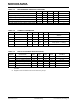
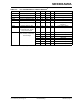
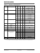
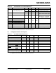
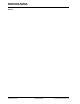

Table Of Contents
- Features
- Operational
- RF/Analog Features
- Media Access Controller (MAC)/ Baseband Features
- Pin diagram
- Table of Contents
- Most Current Data Sheet
- Errata
- Customer Notification System
- 1.0 Device Overview
- 2.0 Circuit Description
- 3.0 Regulatory Approval
- 4.0 Electrical Characteristics
- Appendix A: Revision History
- Product Identification System
- Corporate Office
- Atlanta
- Boston
- Chicago
- Cleveland
- Fax: 216-447-0643
- Dallas
- Detroit
- Indianapolis
- Toronto
- Fax: 852-2401-3431
- Australia - Sydney
- China - Beijing
- China - Shanghai
- India - Bangalore
- Korea - Daegu
- Korea - Seoul
- Singapore
- Taiwan - Taipei
- Fax: 43-7242-2244-393
- Denmark - Copenhagen
- France - Paris
- Germany - Munich
- Italy - Milan
- Spain - Madrid
- UK - Wokingham
- Worldwide Sales and Service

MRF89XAM9A
DS00000A-page 22 Preliminary © 2011 Microchip Technology Inc.
TABLE 4-1: RECOMMENDED OPERATING CONDITIONS
TABLE 4-2: CURRENT CONSUMPTION
TABLE 4-3: DIGITAL I/O PIN INPUT SPECIFICATIONS
(1)
Parameter Min Typ Max Unit Condition
Ambient Operating Temperature -40 — +85 °C —
Supply Voltage for RF, Analog and Digital Circuits 2.1 — 3.6 V —
Supply Voltage for Digital I/O 2.1 — 3.6 V —
Input High Voltage (V
IH) 0.5 * VIN —VIN + 0.3 V —
Input Low Voltage (VIL) -0.3V — 0.2 * VIN V—
AC Peak Voltage on Open Collector Outputs (IO)
(1)
VIN – 1.5 — VIN + 1.5 V —
Note 1: At minimum, V
IN – 1.5V should not be lower than 1.8V.
Symbol Chip Mode Min Typ Max Unit Condition
I
DDSL Sleep — 0.1 2 µA Sleep clock disabled, all blocks
disabled
I
DDST Idle — 65 80 µA Oscillator and baseband enabled
IDDFS Frequency Synthesizer — 1.3 1.7 mA Frequency synthesizer running
I
DDTX Tx —
—
25
16
30
21
mA
mA
Output power = +10 dBm
Output power = +1 dBm
(1)
IDDRX Rx — 3.0 3.5 mA —
Note 1: Guaranteed by design and characterization.
Symbol Characteristic Min Typ Max Unit Condition
V
IL Input Low Voltage — — 0.2 * VIN V—
V
IH Input High Voltage 0.8 * VIN ——V —
IIL Input Low Leakage Current
(2)
-0.5 — 0.5 µA VIL = 0V
I
IH Input High Leakage Current -0.5 — 0.5 µA VIH = VIN, VIN = 3.7
V
OL Digital Low Output Voltage — — 0.1 * VIN —IOL = 1 mA
V
OH Digital Low Output 0.9 * VIN ——V IOH = -1 mA
Note 1: Measurement Conditions: T
A = 25°C, VIN = 3.3V, Crystal Frequency = 12.8 MHz, unless otherwise
specified.
2: Negative current is defined as the current sourced by the pin.