
User Manual
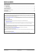


Table Of Contents
- Features:
- Operational:
- RF/Analog Features:
- MAC/Baseband Features:
- Pin Diagram:
- Table of Contents
- Most Current Data Sheet
- Errata
- Customer Notification System
- 1.0 Device Overview
- 2.0 Circuit Description
- 3.0 Regulatory Approval
- 4.0 Electrical Characteristics
- Appendix A: Revision History
- The Microchip Web Site
- Customer Change Notification Service
- Customer Support
- Reader Response
- Product Identification System

© 2011 Microchip Technology Inc. Preliminary DS00000A-page 7
MRF24J40MC
1.3 Operation
The MRF24J40MC module is based on the Microchip
Technology MRF24J40 2.4 GHz IEEE 802.15.4 RF
Transceiver IC. Serial communication and
configuration are documented in the “MRF24J40 Data
Sheet” (DS39776).
This section emphasizes operational settings that are
unique to the MRF24J40MC module design that must
be followed for proper operation.
1.3.1 PA/LNA CONTROL
Operation of the PA U3 and LNA U2 is controlled by the
MRF24J40 internal RF state machine through RF
switches, U1 and U4, and the GPIO1 and GPIO2 pins on
the MRF24J40. Figure 1-5 shows the PA/LNA block
diagram. Figure 2-2 is the schematic diagram for the
module.
The internal RF state machine is configured for the PA/
LNA mode by setting TESTMODE (0x22<2:0>) = 111.
Pins GPIO1 and GPIO2 control the RF switches, PA
and LNA automatically when the MRF24J40 receives
and transmits data.
Voltage regulator U5 supplies a regulated 2.2V to the
PA. This provides a stable voltage to the PA over the V
IN
voltage range of the module. U5 is enabled or shutdown
from GPIO3. Ensure that the GPIO3 direction has been
set to output (TRISGP3 (0x34<3>) = 1). Setting a logic
high (GPIO3 (0x33<3>) = 1) enables the voltage
regulator and supplies voltage to the PA. Setting a logic
low (GPIO3 (0x33<3>) = 0) will shutdown the voltage
regulator, disabling the PA, and provides the lowest
shutdown current.
FIGURE 1-5: PA/LNA BLOCK DIAGRAM
Note: A complete explanation of the operation of
the PA/LNA control is documented in the
“MRF24J40 Data Sheet” (DS39776),
Section 4.2 “External PA/LNA Control”.
MRF24J40
GPIO1
GPIO2
U.FL
Connector
Balun
RFP
RFN
PA
uPG2250T5N
LNA
PA
RF Switch
UPG2179TB
RF Switch
UPG2179TB
LNA
uPC8233TK
V2 V1
V2 V1
GPIO3
Voltage Regulator
TC1187VCT713
V
OUT
SHDN
50 ohm