
User's Manual


Table Of Contents
- Features:
- Operational:
- RF/Analog Features:
- MAC/Baseband Features:
- Table of Contents
- Most Current Data Sheet
- Errata
- Customer Notification System
- 1.0 Device Overview
- 2.0 Microcontroller Interface
- 3.0 Circuit Interface
- 4.0 Regulatory Approval
- 5.0 Electrical Characteristics
- 6.0 Packaging Information
- Appendix A: Revision History
- The Microchip Web Site
- Customer Change Notification Service
- Customer Support
- Reader Response
- MRF24J40MA Product Identification System
MRF24J40MA
DS00000A-page 6 Advance Information © 2008 Microchip Technology Inc.
TABLE 1-1: PIN DESCRIPTION
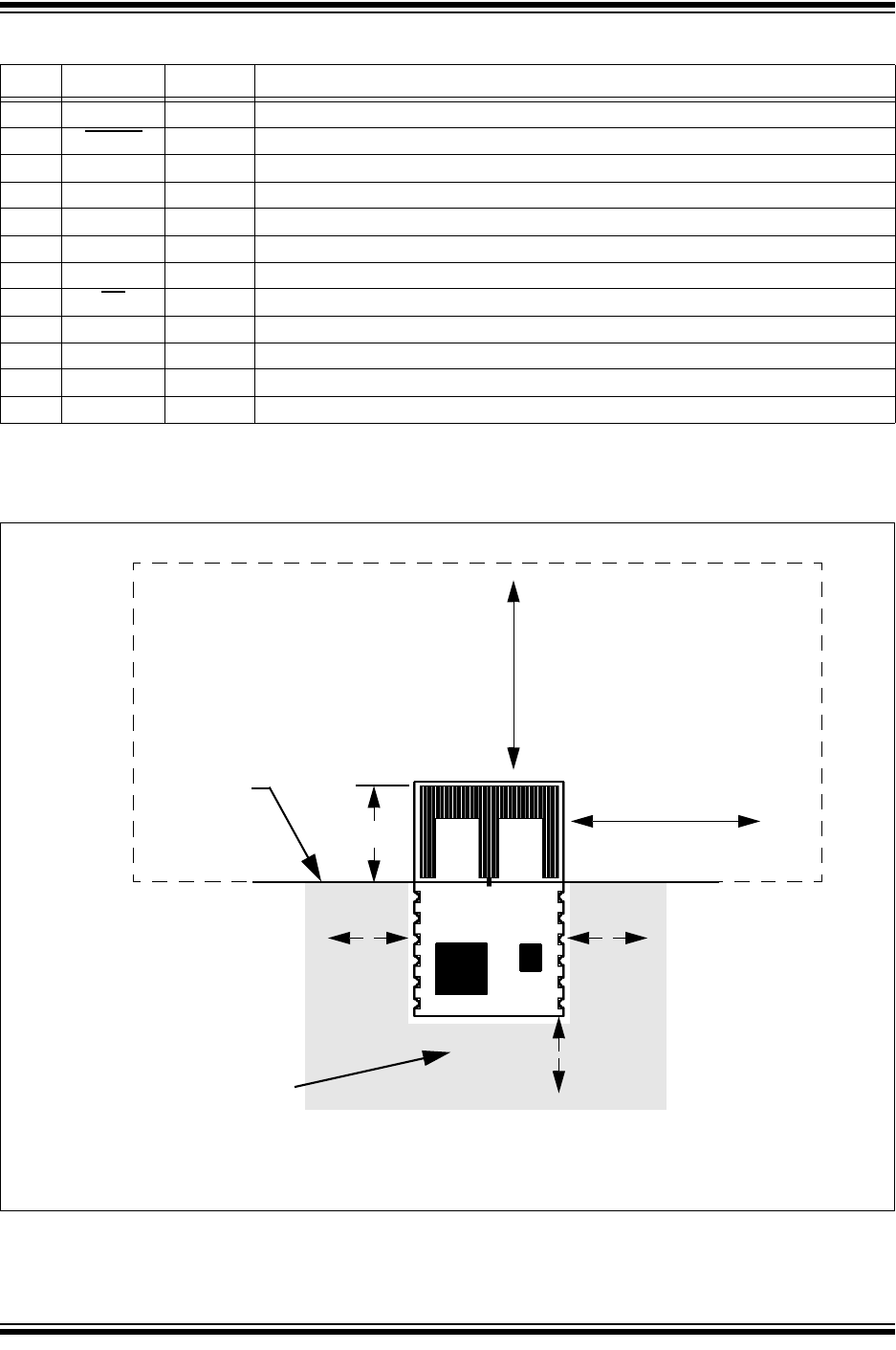
FIGURE 1-2: MOUNTING DETAILS
Pin Symbol Type Description
1 GND Power
Ground
2 RESET
DI Global hardware reset pin
3 WAKE DI External wake-up trigger
4 INT DO Interrupt pin to microcontroller
5 SDI DI Serial interface data input
6 SCK DI Serial interface clock
7 SDO DO Serial interface data output from MRF24J40
8CS
DI Serial interface enable
9 CLKOUT DO 20/10/5/2.5 MHz clock output
10 V
IN Power Power supply
11 GND Ground Ground
12 GND Ground Ground
Legend: Pin type abbreviation: A = Analog, D = Digital, I = Input, O = Output
0.470”
Edge of PCB
Keep area around antenna
(approximately 1.2 inches)
clear of metalic structures
for best performance
PCB Ground Plane (Counterpoise)
Extend as far as possible to
the sides and below the module
(at least 0.4 inches on each side)
for best performance
0.4”
0.4” 0.4”
1.2”
1.2”