
Datasheet

MCP9501/2/3/4
DS22268A-page 4 © 2011 Microchip Technology Inc.
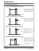
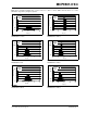
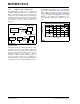
2.0 TYPICAL PERFORMANCE CURVES
Note: Unless otherwise indicated, V
DD
= 2.7V to 5.5V, T
A
= -40°C to +125°C, GND = Ground, R
PULL-UP
= 10 kΩ
(MCP9501/3 only) and 0.1 µF bypass capacitor.
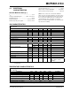
FIGURE 2-1: Temperature Accuracy.
FIGURE 2-2: Hysteresis vs. Temperature.
FIGURE 2-3: Supply Current vs.
Temperature.
FIGURE 2-4: Leakage vs. Temperature.
FIGURE 2-5: V
OL
,V
OH
vs. Temperature.
FIGURE 2-6: Power On Reset Threshold
vs. Temperature.
Note: The graphs and tables provided following this note are a statistical summary based on a limited number of
samples and are provided for informational purposes only. The performance characteristics listed herein
are not tested or guaranteed. In some graphs or tables, the data presented may be outside the specified
operating range (e.g., outside specified power supply range) and therefore outside the warranted range.
-6.0
-4.0
-2.0
0.0
2.0
4.0
6.0
-40-200 20406080100120
T
A
(°C)
Temperature Accuracy (°C)
Spec. Limits
+ St. Dev.
Average
- St. Dev.
V
DD
= 4.1V
32 units
0.0
0.5
1.0
1.5
2.0
2.5
3.0
3.5
4.0
-40-200 20406080100120
T
A
(°C)
HYST = V
SS
, Hysteresis (°C)
6.0
7.0
8.0
9.0
10.0
11.0
12.0
13.0
14.0
HYST = V
DD
, Hysteresis (°C)
HYST = V
SS
HYST = V
DD
10
15
20
25
30
35
40
-40-200 20406080100120
T
A
(°C)
I
DD
(µA)
V
DD
= 5.5
V
V
DD
= 4.1
V
V
DD
= 2.7
V
0.00
0.02
0.04
0.06
0.08
0.10
-40-200 20406080100120
T
A
(°C)
Leakage (µA)
HYST Input Pin
Open-Drain Output
(MCP9501/03 only)
0%
5%
10%
15%
20%
-40-200 20406080100120
T
A
(°C)
V
OL
(% of V
DD
)
80%
85%
90%
95%
100%
V
OH
(% of V
DD
)
V
OH
, V
DD
= 5.5
V
V
OH
, V
DD
= 4.1
V
V
OH
, V
DD
= 2.7
V
V
OL
, V
DD
= 5.5
V
V
OL
, V
DD
= 4.1
V
V
OL
, V
DD
= 2.7
V
V
POR
Hysteresis (mV)
45
55
65
75
85
95
105
0.0
0.5
1.0
1.5
2.0
2.5
3.0
-40 -20 0 20 40 60 80 100 120
V
P
O
R
H
y
s
t
e
r
e
s
i
s
(
m
V
)
V
P
O
R
(
V
)
T
A
(°C)
V
POR
Hysteresis
V
POR
(V)
V
POR
Hysteresis (mV)