
Datasheet


2010-2014 Microchip Technology Inc. DS20005010F-page 5
MCP7940N
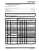
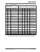
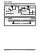
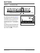
TABLE 1-2: AC CHARACTERISTICS
AC CHARACTERISTICS
Electrical Characteristics:
Industrial (I): VCC = +1.8V to 5.5V TA = -40°C to +85°C
Extended (E): V
CC = +1.8V to 5.5V TA = -40°C to +125°C
Param.
No.
Symbol Characteristic Min. Typ. Max. Units Conditions
1F
CLK Clock frequency —
—
—
—
100
400
kHz 1.8V VCC < 2.5V
2.5V V
CC 5.5V
2THIGH Clock high time 4000
600
—
—
—
—
ns 1.8V VCC < 2.5V
2.5V V
CC 5.5V
3TLOW Clock low time 4700
1300
—
—
—
—
ns 1.8V VCC < 2.5V
2.5V V
CC 5.5V
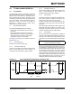
4T
R SDA and SCL rise time
(Note 1)
—
—
—
—
1000
300
ns 1.8V VCC < 2.5V
2.5V V
CC 5.5V
5TF SDA and SCL fall time
(Note 1)
—
—
—
—
1000
300
ns 1.8V VCC < 2.5V
2.5V V
CC 5.5V
6THD:STA Start condition hold time 4000
600
—
—
—
—
ns 1.8V VCC < 2.5V
2.5V V
CC 5.5V
7T
SU:STA Start condition setup time 4700
600
—
—
—
—
ns 1.8V VCC < 2.5V
2.5V V
CC 5.5V
8THD:DAT Data input hold time 0 — — ns (Note 2)
9T
SU:DAT Data input setup time 250
100
—
—
—
—
ns 1.8V VCC < 2.5V
2.5V V
CC 5.5V
10 TSU:STO Stop condition setup time 4000
600
—
—
—
—
ns 1.8V VCC < 2.5V
2.5V V
CC 5.5V
11 TAA Output valid from clock —
—
—
—
3500
900
ns 1.8V VCC < 2.5V
2.5V V
CC 5.5V
12 T
BUF Bus free time: Time the bus
must be free before a new
transmission can start
4700
1300
—
—
—
—
ns 1.8V V
CC < 2.5V
2.5V V
CC 5.5V
13 T
SP Input filter spike suppression
(SDA and SCL pins)
— — 50 ns (Note 1)
14 T
FVCC VCC fall time 300 — — s (Note 1)
15 T
RVCC VCC rise time 0 — — s (Note 1)
16 FOSC Oscillator frequency — 32.768 — kHz —
17 TOSF Oscillator timeout period 1 — — ms (Note 1)
Note 1: Not 100% tested.
2: As a transmitter, the device must provide an internal minimum delay time to bridge the undefined region
(minimum 300 ns) of the falling edge of SCL to avoid unintended generation of Start or Stop conditions.