
Datasheet


2010-2014 Microchip Technology Inc. DS20005010F-page 35
MCP7940N
6.0 ON-BOARD MEMORY
The MCP7940N has 64 bytes of SRAM for general pur-
pose usage. It is retained when the primary power
supply is removed if a backup supply is present and
enabled.
Although the SRAM is a separate block from the RTCC
registers, they are accessed using the same control
byte, ‘1101111X’.
6.1 SRAM/RTCC Registers
The RTCC registers are located at addresses 0x00 to
0x1F, and the SRAM is located at addresses 0x20 to
0x5F. The SRAM can be accessed while the RTCC reg-
isters are being internally updated. The SRAM is not
initialized by a Power-On Reset (POR).
Neither the RTCC registers nor the SRAM can be
accessed when the device is operating off the backup
power supply.
6.1.1 SRAM/RTCC REGISTER BYTE
WRITE
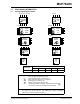
Following the Start condition from the master, the con-
trol code and the R/W
bit (which is a logic low) are
clocked onto the bus by the master transmitter. This
indicates to the addressed slave receiver that the
address byte will follow after it has generated an
Acknowledge bit during the ninth clock cycle. There-
fore, the next byte transmitted by the master is the
address and will be written into the Address Pointer of
the MCP7940N. After receiving another Acknowledge
bit from the MCP7940N, the master device transmits
the data byte to be written into the addressed memory
location. The MCP7940N stores the data byte into
memory and acknowledges again, and the master gen-
erates a Stop condition (Figure 6-1).
If an attempt is made to write to an address past 0x5F,
the MCP7940N will not acknowledge the address or
data bytes, and no data will be written. After a byte
Write command, the internal Address Pointer will point
to the address location following the one that was just
written.
6.1.2 SRAM/RTCC REGISTER
SEQUENTIAL WRITE
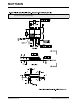
The write control byte, address, and the first data byte
are transmitted to the MCP7940N in the same way as
in a byte write. But instead of generating a Stop condi-
tion, the master transmits additional data bytes. Upon
receipt of each byte, the MCP7940N responds with an
Acknowledge, during which the data is latched into
memory and the Address Pointer is internally incre-
mented by one. As with the byte write operation, the
master ends the command by generating a Stop condi-
tion (Figure 6-2).
There is no limit to the number of bytes that can be writ-
ten in a single command. However, because the RTCC
registers and SRAM are separate blocks, writing past
the end of each block will cause the Address Pointer to
roll over to the beginning of the same block. Specifi-
cally, the Address Pointer will roll over from 0x1F to
0x00, and from 0x5F to 0x20.
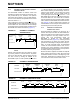
FIGURE 6-1: SRAM/RTCC BYTE WRITE
FIGURE 6-2: SRAM/RTCC SEQUENTIAL WRITE
BUS ACTIVITY
MASTER
SDA LINE
BUS ACTIVITY
S
T
A
R
T
CONTROL
BYTE
ADDRESS
BYTE
DATA
S
T
O
P
A
C
K
A
C
K
A
C
K
S 1101 01
11 P0
BUS ACTIVITY
MASTER
SDA LINE
BUS ACTIVITY
S
T
A
R
T
CONTROL
BYTE
ADDRESS
BYTE
DATA BYTE 0
S
T
O
P
A
C
K
A
C
K
A
C
K
DATA BYTE N
A
C
K
S
1101 0
111
P
0