
Datasheet

2010-2014 Microchip Technology Inc. DS20005010F-page 3
MCP7940N
1.0 ELECTRICAL CHARACTERISTICS
Absolute Maximum Ratings
(†)
VCC.............................................................................................................................................................................6.5V
All inputs and outputs (except SDA and SCL) w.r.t. V
SS.....................................................................-0.6V to VCC +1.0V
SDA and SCL w.r.t. V
SS ............................................................................................................................... -0.6V to 6.5V
Storage temperature ...............................................................................................................................-65°C to +150°C
Ambient temperature with power applied................................................................................................-40°C to +125°C
ESD protection on all pins 4 kV
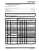
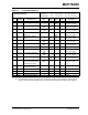
TABLE 1-1: DC CHARACTERISTICS
† NOTICE: Stresses above those listed under “Absolute Maximum Ratings” may cause permanent damage to the
device. This is a stress rating only and functional operation of the device at those or any other conditions above those
indicated in the operational listings of this specification is not implied. Exposure to maximum rating conditions for
extended periods may affect device reliability.
DC CHARACTERISTICS
Electrical Characteristics:
Industrial (I): VCC = +1.8V to 5.5V TA = -40°C to +85°C
Extended (E): V
CC = +1.8V to 5.5V TA = -40°C to +125°C
Param.
No.
Sym. Characteristic Min. Typ.
(2)
Max. Units Conditions
D1 V
IH High-level input voltage 0.7 VCC ——V—
D2 VIL Low-level input voltage — — 0.3 VCC
0.2 VCC
V
V
VCC 2.5V
V
CC < 2.5V
D3 V
HYS Hysteresis of Schmitt
Trigger inputs
(SDA, SCL pins)
0.05
V
CC
—— V(Note 1)
D4 VOL Low-level output voltage
(MFP, SDA pins)
——0.40VIOL = 3.0 mA @ VCC = 4.5V
I
OL = 2.1 mA @ VCC = 2.5V
D5 ILI Input leakage current — — ±1 AVIN = VSS or VCC
D6 ILO Output leakage current — — ±1 AVOUT = VSS or VCC
D7 CIN,
C
OUT
Pin capacitance
(SDA, SCL, MFP pins)
— — 10 pF VCC = 5.0V (Note 1)
T
A = 25°C, f = 1 MHz
D8 C
OSC Oscillator pin
capacitance (X1, X2 pins)
—3—pF(Note 1)
D9 I
CCREAD SRAM/RTCC register
operating current
——300AVCC = 5.5V, SCL = 400 kHz
I
CCWRITE ——400AVCC = 5.5V, SCL = 400 kHz
D10 ICCDAT VCC data-retention
current (oscillator off)
——1A SCL, SDA, VCC = 5.5V (I-Temp)
——5A SCL, SDA, VCC = 5.5V (E-temp)
D11 I
CCT Timekeeping current — 1.2 — AVCC = 3.3V (Note 1)
D12 VTRIP Power-fail switchover
voltage
1.3 1.5 1.7 V —
D13 V
BAT Backup supply voltage
range
1.3 — 5.5 V (Note 1)
D14 I
BATT Timekeeping backup
current
——
925
850
1200
9000
nA
nA
nA
VBAT = 1.3V, VCC = VSS (Note 1)
V
BAT = 3.0V, VCC = VSS (Note 1)
V
BAT = 5.5V, VCC = VSS (Note 1)
Note 1: This parameter is not tested but ensured by characterization.
2: Typical measurements taken at room temperature.