
Datasheet

2010-2014 Microchip Technology Inc. DS20005010F-page 13
MCP7940N
5.2 Oscillator Configuration
The MCP7940N can be operated in two different oscil-
lator configurations: using an external crystal or using
an external clock input.
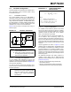
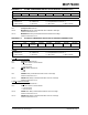
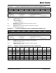
5.2.1 EXTERNAL CRYSTAL
The crystal oscillator circuit on the MCP7940N is
designed to operate with a standard 32.768 kHz tuning
fork crystal and matching external load capacitors. By
using external load capacitors, the MCP7940N allows
for a wide selection of crystals. Suitable crystals have a
load capacitance (C
L) of 6-9 pF. Crystals with a load
capacitance of 12.5 pF are not recommended.
Figure 5-2 shows the pin connections when using an
external crystal.
FIGURE 5-2: CRYSTAL OPERATION
5.2.1.1 Choosing Load Capacitors
CL is the effective load capacitance as seen by the
crystal, and includes the physical load capacitors, pin
capacitance, and stray board capacitance. Equation 5-1
can be used to calculate C
L.
C
X1
and C
X2
are the external load capacitors. They
must be chosen to match the selected crystal’s speci-
fied load capacitance.
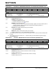
EQUATION 5-1: LOAD CAPACITANCE
CALCULATION
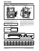
5.2.1.2 Layout Considerations
The oscillator circuit should be placed on the same
side of the board as the device. Place the oscillator
circuit close to the respective oscillator pins. The load
capacitors should be placed next to the oscillator
itself, on the same side of the board.
Use a grounded copper pour around the oscillator cir-
cuit to isolate it from surrounding circuits. The
grounded copper pour should be routed directly to V
SS.
Do not run any signal traces or power traces inside the
ground pour. Also, if using a two-sided board, avoid any
traces on the other side of the board where the crystal
is placed.
Layout suggestions are shown in Figure 5-3. In-line
packages may be handled with a single-sided layout
that completely encompasses the oscillator pins. With
fine-pitch packages, it is not always possible to com-
pletely surround the pins and components. A suitable
solution is to tie the broken guard sections to a mirrored
ground layer. In all cases, the guard trace(s) must be
returned to ground.
For additional information and design guidance on
oscillator circuits, please refer to these Microchip
Application Notes, available at the corporate web site
(www.microchip.com):
• AN1365, “Recommended Usage of Microchip
Serial RTCC Devices”
• AN1519, “Recommended Crystals for Microchip
Stand-Alone Real-Time Clock Calendar Devices”
Note 1: The ST bit must be set to enable the
crystal oscillator circuit.
2: Always verify oscillator performance over
the voltage and temperature range that is
expected for the application.
Note: If the load capacitance is not correctly
matched to the chosen crystal’s specified
value, the crystal may give a frequency
outside of the crystal manufacturer’s
specifications.
CX1
CX2
Quartz
X1
ST
To Internal
Logic
Crystal
X2
MCP7940N
CL
C
X1
C
X2
C
X1
C
X2
+
-------------------------- C
STRAY+=
Where:
C
L Effective load capacitance=
C
X1
Capacitor value on X1 COSC+=
C
X2
Capacitor value on X2 COSC+=
C
STRAY PCB stray capacitance=