
Datasheet

MCP7940N
DS20005010F-page 10 2010-2014 Microchip Technology Inc.
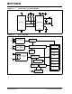
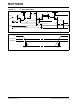
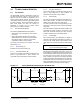
FIGURE 4-2: ACKNOWLEDGE TIMING
4.1.2 DEVICE ADDRESSING
The control byte is the first byte received following the
Start condition from the master device (Figure 4-3).
The control byte begins with a 4-bit control code. For
the MCP7940N, this is set ‘1101’ for register read and
write operations. The next three bits are non-config-
urable Chip Select bits that must always be set to ‘1’.
The last bit of the control byte defines the operation to
be performed. When set to a ‘1’ a read operation is
selected, and when set to a ‘0’ a write operation is
selected.
The combination of the 4-bit control code and the three
Chip Select bits is called the slave address. Upon
receiving a valid slave address, the slave device out-
puts an acknowledge signal on the SDA line. Depend-
ing on the state of the R/W
bit, the MCP7940N will
select a read or a write operation.
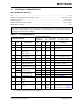
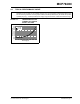
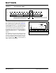
FIGURE 4-3: CONTROL BYTE FORMAT
SCL
987654321123
Transmitter must release the SDA line at this point
allowing the Receiver to pull the SDA line low to
acknowledge the previous eight bits of data.
Receiver must release the SDA line at this point
so the Transmitter can continue sending data.
Data from transmitter
Data from transmitter
SDA
Acknowledge
Bit
1101111SACKR/W
Control Code
Chip Select
Bits
Acknowledge Bit
Start Bit
Read/Write
Bit
RTCC Register/SRAM Control Byte