MCP7940N Battery-Backed I2C™ Real-Time Clock/Calendar with SRAM Timekeeping Features: Operating Ranges: • Real-Time Clock/Calendar (RTCC): - Hours, Minutes, Seconds, Day of Week, Day, Month, Year - Leap year compensated to 2399 - 12/24 hour modes • Oscillator for 32.
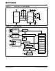
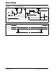
MCP7940N FIGURE 1-1: TYPICAL APPLICATION SCHEMATIC VCC VCC VCC 8 VCC 6 PIC® MCU 5 7 SCL MCP7940N 2 SDA X2 MFP VBAT VBAT BLOCK DIAGRAM VCC Power Control and Switchover VSS VBAT SCL SDA CX2 3 VSS 4 FIGURE 1-2: CX1 1 32.768 KHZ X1 Power-Fail Time-Stamp Control Logic I2C™ Interface and Addressing Configuration Seconds SRAM Minutes X1 32.
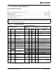
MCP7940N 1.0 ELECTRICAL CHARACTERISTICS Absolute Maximum Ratings (†) VCC.............................................................................................................................................................................6.5V All inputs and outputs (except SDA and SCL) w.r.t. VSS .....................................................................-0.6V to VCC +1.0V SDA and SCL w.r.t. VSS ..............................................................................................
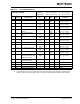
MCP7940N DC CHARACTERISTICS (Continued) Param. No. D15 Note 1: 2: Sym. Characteristic IBATDAT VBAT data retention current (oscillator off) Electrical Characteristics: Industrial (I): VCC = +1.8V to 5.5V Extended (E): VCC = +1.8V to 5.5V Min. Typ.(2) Max. Units — — 750 nA TA = -40°C to +85°C TA = -40°C to +125°C Conditions VBAT = 3.6V, VCC = VSS This parameter is not tested but ensured by characterization. Typical measurements taken at room temperature.
MCP7940N TABLE 1-2: AC CHARACTERISTICS Electrical Characteristics: Industrial (I): VCC = +1.8V to 5.5V Extended (E): VCC = +1.8V to 5.5V AC CHARACTERISTICS Param. Symbol No. Characteristic Min. Typ. Max. Units TA = -40°C to +85°C TA = -40°C to +125°C Conditions 1 FCLK Clock frequency — — — — 100 400 kHz 1.8V VCC < 2.5V 2.5V VCC 5.5V 2 THIGH Clock high time 4000 600 — — — — ns 1.8V VCC < 2.5V 2.5V VCC 5.5V 3 TLOW Clock low time 4700 1300 — — — — ns 1.8V VCC < 2.
MCP7940N I2C BUS TIMING DATA FIGURE 1-3: 5 SCL 7 SDA In D3 2 3 8 9 4 10 6 13 12 11 SDA Out FIGURE 1-4: POWER SUPPLY TRANSITION TIMING VCC VTRIP(MAX) VTRIP(MIN) 14 DS20005010F-page 6 15 2010-2014 Microchip Technology Inc.
MCP7940N 2.0 TYPICAL PERFORMANCE CURVE Note: The graphs and tables provided following this note are a statistical summary based on a limited number of samples and are provided for informational purposes only. The performance characteristics listed herein are not tested or guaranteed. In some graphs or tables, the data represented may be outside the specified operating range (e.g., outside specified power supply range) and therefore, outside the warranted range. IBATT Current (µA) FIGURE 2-1: 5.5 5.
MCP7940N 3.0 PIN DESCRIPTIONS The descriptions of the pins are listed in Table 3-1. TABLE 3-1: Name X1 X2 VBAT Vss SDA SCL MFP Vcc Note: 3.
MCP7940N 4.0 I2C BUS CHARACTERISTICS 4.1.1.3 4.1 I2C Interface A low-to-high transition of the SDA line while the clock (SCL) is high determines a Stop condition. All operations must end with a Stop condition. The MCP7940N supports a bidirectional 2-wire bus and data transmission protocol. A device that sends data onto the bus is defined as transmitter, and a device receiving data as receiver.
MCP7940N FIGURE 4-2: ACKNOWLEDGE TIMING Acknowledge Bit SCL 1 SDA 2 3 4 5 6 7 8 9 1 DEVICE ADDRESSING The control byte is the first byte received following the Start condition from the master device (Figure 4-3). The control byte begins with a 4-bit control code. For the MCP7940N, this is set ‘1101’ for register read and write operations. The next three bits are non-configurable Chip Select bits that must always be set to ‘1’.
MCP7940N 5.0 FUNCTIONAL DESCRIPTION 5.1 The MCP7940N is a highly-integrated Real-Time Clock/Calendar (RTCC). Using an on-board, lowpower oscillator, the current time is maintained in seconds, minutes, hours, day of week, date, month, and year. The MCP7940N also features 64 bytes of general purpose SRAM. Two alarm modules allow interrupts to be generated at specific times with flexible comparison options. Digital trimming can be used to compensate for inaccuracies inherent with crystals.
MCP7940N TABLE 5-1: DETAILED RTCC REGISTER MAP Addr. Register Name Bit 7 Bit 6 Bit 5 Bit 4 Bit 3 Bit 2 Bit 1 Bit 0 Section 5.
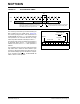
MCP7940N 5.2 Oscillator Configuration EQUATION 5-1: The MCP7940N can be operated in two different oscillator configurations: using an external crystal or using an external clock input. 5.2.1 Figure 5-2 shows the pin connections when using an external crystal. FIGURE 5-2: CRYSTAL OPERATION MCP7940N X1 CX 1 To Internal Logic Quartz Crystal CX 2 ST X2 Note 1: The ST bit must be set to enable the crystal oscillator circuit.
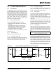
MCP7940N FIGURE 5-3: SUGGESTED PLACEMENT OF THE OSCILLATOR CIRCUIT Single-Sided and In-line Layouts: Copper Pour (tied to ground) Fine-Pitch (Dual-Sided) Layouts: Oscillator Crystal Top Layer Copper Pour (tied to ground) Bottom Layer Copper Pour (tied to ground) X1 X1 CX1 CX1 X2 GND CX2 Oscillator Crystal GND CX2 ` X2 DEVICE PINS DEVICE PINS 5.2.2 5.2.3 EXTERNAL CLOCK INPUT A 32.768 kHz external clock source can be connected to the X1 pin (Figure 5-4).
MCP7940N 5.3 Timekeeping The MCP7940N maintains the current time and date using an external 32.768 kHz crystal or clock source. Separate registers are used for tracking seconds, minutes, hours, day of week, date, month, and year. The MCP7940N automatically adjusts for months with less than 31 days and compensates for leap years from 2001 to 2399. The year is stored as a two-digit value. Both 12-hour and 24-hour time formats are supported and are selected using the 12/24 bit.
MCP7940N REGISTER 5-1: RTCSEC: TIMEKEEPING SECONDS VALUE REGISTER (ADDRESS 0x00) R/W-0 R/W-0 R/W-0 R/W-0 R/W-0 R/W-0 R/W-0 R/W-0 ST SECTEN2 SECTEN1 SECTEN0 SECONE3 SECONE2 SECONE1 SECONE0 bit 7 bit 0 Legend: R = Readable bit W = Writable bit U = Unimplemented bit, read as ‘0’ -n = Value at POR ‘1’ = Bit is set ‘0’ = Bit is clear x = Bit is unknown bit 7 ST: Start Oscillator bit 1 = Oscillator enabled 0 = Oscillator disabled bit 6-4 SECTEN<2:0>: Binary-Coded Decimal Value of Sec
MCP7940N REGISTER 5-2: RTCMIN: TIMEKEEPING MINUTES VALUE REGISTER (ADDRESS 0x01) U-0 R/W-0 R/W-0 R/W-0 R/W-0 R/W-0 R/W-0 R/W-0 — MINTEN2 MINTEN1 MINTEN0 MINONE3 MINONE2 MINONE1 MINONE0 bit 7 bit 0 Legend: R = Readable bit W = Writable bit U = Unimplemented bit, read as ‘0’ -n = Value at POR ‘1’ = Bit is set ‘0’ = Bit is clear x = Bit is unknown bit 7 Unimplemented: Read as ‘0’ bit 6-4 MINTEN<2:0>: Binary-Coded Decimal Value of Minute’s Tens Digit Contains a value from 0 to 5 b
MCP7940N REGISTER 5-4: RTCWKDAY: TIMEKEEPING WEEKDAY VALUE REGISTER (ADDRESS 0x03) U-0 U-0 R-0 R/W-0 R/W-0 R/W-0 R/W-0 R/W-1 — — OSCRUN PWRFAIL VBATEN WKDAY2 WKDAY1 WKDAY0 bit 7 bit 0 Legend: R = Readable bit W = Writable bit U = Unimplemented bit, read as ‘0’ -n = Value at POR ‘1’ = Bit is set ‘0’ = Bit is clear x = Bit is unknown bit 7-6 Unimplemented: Read as ‘0’ bit 5 OSCRUN: Oscillator Status bit 1 = Oscillator is enabled and running 0 = Oscillator has stopped or has been
MCP7940N REGISTER 5-6: RTCMTH: TIMEKEEPING MONTH VALUE REGISTER (ADDRESS 0x05) U-0 U-0 R-0 R/W-0 R/W-0 R/W-0 R/W-0 R/W-1 — — LPYR MTHTEN0 MTHONE3 MTHONE2 MTHONE1 MTHONE0 bit 7 bit 0 Legend: R = Readable bit W = Writable bit U = Unimplemented bit, read as ‘0’ -n = Value at POR ‘1’ = Bit is set ‘0’ = Bit is clear x = Bit is unknown bit 7-6 Unimplemented: Read as ‘0’ bit 5 LPYR: Leap Year bit 1 = Year is a leap year 0 = Year is not a leap year bit 4 MTHTEN0: Binary-Coded Decimal
MCP7940N 5.4 Alarms TABLE 5-5: ALARM MASKS The MCP7940N features two independent alarms. Each alarm can be used to either generate an interrupt at a specific time in the future, or to generate a periodic interrupt every minute, hour, day, day of week, or month. ALMxMSK<2:0> Alarm Asserts on Match of 000 Seconds 001 Minutes 010 Hours There is a separate interrupt flag, ALMxIF, for each alarm. The interrupt flags are set by hardware when the chosen alarm mask condition matches (Table 5-5).
MCP7940N 5.4.1 CONFIGURING THE ALARM In order to configure the alarm modules, the following steps need to be performed: 1. 2. 3. 4. 5. 6.
MCP7940N REGISTER 5-10: ALMxHOUR: ALARM0/1 HOURS VALUE REGISTER (ADDRESSES 0x0C/0x13) U-0 R-0 R/W-0 R/W-0 R/W-0 R/W-0 R/W-0 R/W-0 — 12/24 AM/PM HRTEN1 HRTEN0 HRONE3 HRONE2 HRONE1 HRONE0 bit 7 bit 0 Legend: R = Readable bit W = Writable bit U = Unimplemented bit, read as ‘0’ -n = Value at POR ‘1’ = Bit is set ‘0’ = Bit is clear x = Bit is unknown If 12/24 = 1 (12-hour format): bit 7 Unimplemented: Read as ‘0’ bit 6 12/24: 12 or 24 Hour Time Format bit(1) 1 = 12-hour format 0 = 2
MCP7940N REGISTER 5-11: ALMxWKDAY: ALARM0/1 WEEKDAY VALUE REGISTER (ADDRESSES 0x0D/ 0x14) R/W-0 R/W-0 R/W-0 R/W-0 R/W-0 R/W-0 R/W-0 R/W-1 ALMPOL ALMxMSK2 ALMxMSK1 ALMxMSK0 ALMxIF WKDAY2 WKDAY1 WKDAY0 bit 7 bit 0 Legend: R = Readable bit W = Writable bit U = Unimplemented bit, read as ‘0’ -n = Value at POR ‘1’ = Bit is set ‘0’ = Bit is clear x = Bit is unknown bit 7 ALMPOL: Alarm Interrupt Output Polarity bit 1 = Asserted output state of MFP is a logic high level 0 = Asserted outp
MCP7940N REGISTER 5-13: ALMxMTH: ALARM0/1 MONTH VALUE REGISTER (ADDRESSES 0x0F/0x16) U-0 U-0 U-0 R/W-0 R/W-0 R/W-0 R/W-0 R/W-1 — — — MTHTEN0 MTHONE3 MTHONE2 MTHONE1 MTHONE0 bit 7 bit 0 Legend: R = Readable bit W = Writable bit U = Unimplemented bit, read as ‘0’ -n = Value at POR ‘1’ = Bit is set ‘0’ = Bit is clear x = Bit is unknown bit 7-5 Unimplemented: Read as ‘0’ bit 4 MTHTEN0: Binary-Coded Decimal Value of Month’s Tens Digit Contains a value of 0 or 1 bit 3-0 MTHONE<3:0>
MCP7940N 5.5 Output Configurations TABLE 5-7: SQWEN ALM0EN ALM1EN The MCP7940N features Square Wave Clock Output, Alarm Interrupt Output, and General Purpose Output modes. All of the output functions are multiplexed onto MFP according to Table 5-7. Only the alarm interrupt outputs are available while operating from the backup power supply. If none of the output functions are being used, the MFP can safely be left floating.
MCP7940N REGISTER 5-14: CONTROL: RTCC CONTROL REGISTER (ADDRESS 0x07) R/W-1 R/W-0 R/W-0 R/W-0 R/W-0 R/W-0 R/W-0 R/W-0 OUT SQWEN ALM1EN ALM0EN EXTOSC CRSTRIM SQWFS1 SQWFS0 bit 7 bit 6 bit 5 bit 4 bit 3 bit 2 bit 1 bit 0 Legend: R = Readable bit W = Writable bit U = Unimplemented bit, read as ‘0’ -n = Value at POR ‘1’ = Bit is set ‘0’ = Bit is clear bit 7 x = Bit is unknown OUT: Logic Level for General Purpose Output bit Square Wave Clock Output Mode (SQWEN = 1): Unused.
MCP7940N 5.5.1 SQUARE WAVE OUTPUT MODE The MCP7940N can be configured to generate a square wave clock signal on MFP. The input clock frequency, FOSC, is divided according to the SQWFS<1:0> bits as shown in Table 5-8. The square wave output is not available when operating from the backup power supply. Note: All of the clock output rates are affected by digital trimming except for the 1:1 postscaler value (SQWFS<1:0> = 00). 5.5.2.
MCP7940N TABLE 5-11: SUMMARY OF REGISTERS ASSOCIATED WITH OUTPUT CONFIGURATION Bit 7 Bit 6 Bit 5 Bit 4 Bit 3 Bit 2 Bit 1 Bit 0 Register on Page ALM0WKDAY ALMPOL ALM0MSK2 ALM0MSK1 ALM0MSK0 ALM0IF WKDAY2 WKDAY1 WKDAY0 23 ALM1WKDAY ALMPOL ALM1MSK2 ALM1MSK1 ALM1MSK0 ALM1IF WKDAY2 WKDAY1 WKDAY0 23 OUT SQWEN ALM1EN ALM0EN EXTOSC CRSTRIM SQWFS1 SQWFS0 26 Name CONTROL Legend: — = unimplemented location, read as ‘0’. Shaded cells are not used in output configuration.
MCP7940N 5.6 Digital Trimming The MCP7940N features digital trimming to correct for inaccuracies of the external crystal or clock source, up to roughly ±129 PPM when CRSTRIM = 0. In addition to compensating for intrinsic inaccuracies in the clock, this feature can also be used to correct for error due to temperature variation. This can enable the user to achieve high levels of accuracy across a wide temperature operating range.
MCP7940N 5.6.1 CALIBRATION In order to perform calibration, the number of error clock pulses per minute must be found and the corresponding trim value must be loaded into TRIMVAL<6:0>. There are two methods for determining the trim value. The first method involves measuring an output frequency directly and calculating the deviation from ideal. The second method involves observing the number of seconds gained or lost over a period of time.
MCP7940N 5.6.2 COARSE TRIM MODE When CRSTRIM = 1, Coarse Trim mode is enabled. While in this mode, the MCP7940N will apply trimming at a rate of 128 Hz. If SQWEN is set, the MFP will output a trimmed 64 Hz nominal clock signal. Because trimming is applied at a rate of 128 Hz rather than once every minute, each step of the TRIMVAL<6:0> value has a significantly larger effect on the resulting time deviation and output clock frequency.
MCP7940N 5.7 Battery Backup The MCP7940N features a backup power supply input (VBAT) that can be used to provide power to the timekeeping circuitry, RTCC registers, and SRAM while primary power is unavailable. The MCP7940N will automatically switch to backup power when VCC falls below VTRIP, and back to VCC when it is above VTRIP. 5.7.1 The MCP7940N includes a power-fail time-stamp module that stores the minutes, hours, date, and month when primary power is lost and when it is restored (Figure 5-8).
MCP7940N REGISTER 5-16: PWRxxMIN: POWER-DOWN/POWER-UP TIME-STAMP MINUTES VALUE REGISTER (ADDRESSES 0x18/0x1C) U-0 R/W-0 R/W-0 R/W-0 R/W-0 R/W-0 R/W-0 R/W-0 — MINTEN2 MINTEN1 MINTEN0 MINONE3 MINONE2 MINONE1 MINONE0 bit 7 bit 0 Legend: R = Readable bit W = Writable bit U = Unimplemented bit, read as ‘0’ -n = Value at POR ‘1’ = Bit is set ‘0’ = Bit is clear x = Bit is unknown bit 7 Unimplemented: Read as ‘0’ bit 6-4 MINTEN<2:0>: Binary-Coded Decimal Value of Minute’s Tens Digit Co
MCP7940N REGISTER 5-18: PWRxxDATE: POWER-DOWN/POWER-UP TIME-STAMP DATE VALUE REGISTER (ADDRESSES 0x1A/0x1E) U-0 U-0 R/W-0 — — DATETEN1 R/W-0 R/W-0 DATETEN0 DATEONE3 R/W-0 R/W-0 R/W-0 DATEONE2 DATEONE1 DATEONE0 bit 7 bit 0 Legend: R = Readable bit W = Writable bit U = Unimplemented bit, read as ‘0’ -n = Value at POR ‘1’ = Bit is set ‘0’ = Bit is clear x = Bit is unknown bit 7-6 Unimplemented: Read as ‘0’ bit 5-4 DATETEN<1:0>: Binary-Coded Decimal Value of Date’s Tens Digit Contai
MCP7940N 6.0 ON-BOARD MEMORY bit from the MCP7940N, the master device transmits the data byte to be written into the addressed memory location. The MCP7940N stores the data byte into memory and acknowledges again, and the master generates a Stop condition (Figure 6-1). The MCP7940N has 64 bytes of SRAM for general purpose usage. It is retained when the primary power supply is removed if a backup supply is present and enabled.
MCP7940N 6.1.3 SRAM/RTCC REGISTER CURRENT ADDRESS READ ‘0’). After the address is sent, the master generates a Start condition following the Acknowledge. This terminates the write operation, but not before the internal Address Pointer is set. Then, the master issues the control byte again but with the R/W bit set to a ‘1’. The MCP7940N will then issue an Acknowledge and transmit the 8-bit data word.
MCP7940N 7.0 PACKAGING INFORMATION 7.1 Package Marking Information 8-Lead SOIC (3.
MCP7940N Note: For the most current package drawings, please see the Microchip Packaging Specification located at http://www.microchip.com/packaging DS20005010F-page 38 2010-2014 Microchip Technology Inc.
MCP7940N Note: For the most current package drawings, please see the Microchip Packaging Specification located at http://www.microchip.com/packaging 2010-2014 Microchip Technology Inc.
MCP7940N & ! " #$% ! " # $ % & "' " " ( $ ) % *++&&& ! !+ $ DS20005010F-page 40 2010-2014 Microchip Technology Inc.
MCP7940N & '( ( ) ' * * ! "' % ! " # $ % & "' " " ( $ ) % *++&&& ! !+ $ D N E E1 NOTE 1 1 2 b e c A φ A2 A1 L L1 @ " ! " A ! " E#!7 ) ( " AA 8 8 E E EG H ( G3 K L L 1 1 ; 1 ; L 1; % % ( $ $ "" % )) J; > ? 1 G3 N % 8 % % ( $ N % 81 <
MCP7940N Note: For the most current package drawings, please see the Microchip Packaging Specification located at http://www.microchip.com/packaging DS20005010F-page 42 2010-2014 Microchip Technology Inc.
MCP7940N Note: For the most current package drawings, please see the Microchip Packaging Specification located at http://www.microchip.com/packaging 2010-2014 Microchip Technology Inc.
MCP7940N Note: For the most current package drawings, please see the Microchip Packaging Specification located at http://www.microchip.com/packaging DS20005010F-page 44 2010-2014 Microchip Technology Inc.
MCP7940N Note: For the most current package drawings, please see the Microchip Packaging Specification located at http://www.microchip.com/packaging 2010-2014 Microchip Technology Inc.
MCP7940N Note: For the most current package drawings, please see the Microchip Packaging Specification located at http://www.microchip.com/packaging DS20005010F-page 46 2010-2014 Microchip Technology Inc.
MCP7940N Note: For the most current package drawings, please see the Microchip Packaging Specification located at http://www.microchip.com/packaging 2010-2014 Microchip Technology Inc.
MCP7940N & + , ) - . /0 0 12 ! "'+, % ! " # $ % & "' " " ( $ ) % *++&&& ! !+ $ DS20005010F-page 48 2010-2014 Microchip Technology Inc.
MCP7940N & + # ! " +# % ! " # $ % & "' " " ( $ ) % *++&&& ! !+ $ N NOTE 1 E1 1 3 2 D E A2 A L A1 c e eB b1 b @ " ! " A ! " E#!7 ) ( " E?K8 E E ( H ( EG 1 > ? L L 1 11; 1< 1 ; > " ( 1 1; L L 8 <1 < ; % % ( $ # % $ "" # % N % %
MCP7940N APPENDIX A: REVISION HISTORY Revision A (04/2011) Defined names for all bits and registers, and renamed the bits shown in Table 7-1 for clarification. Renamed the DC characteristics shown in Table 7-2 for clarification. Original release of this document. TABLE 7-1: Revision B (09/2011) • Added Figure 1-2 • Added Parameter D15 to Table 1-1 • Added Section 3.3 “Oscillator Input/Output (X1, X2)”, Section 3.4 “Multifunction Pin (MFP)”, Section 3.
MCP7940N THE MICROCHIP WEB SITE CUSTOMER SUPPORT Microchip provides online support via our WWW site at www.microchip.com. This web site is used as a means to make files and information easily available to customers.
MCP7940N NOTES: DS20005010F-page 52 2010-2014 Microchip Technology Inc.
MCP7940N PRODUCT IDENTIFICATION SYSTEM To order or obtain information, e.g., on pricing or delivery, refer to the factory or the listed sales office. Not every possible ordering combination is listed below. PART NO. Device Device: X /XX Temperature Package Range MCP7940N = MCP7940NT= 1.8V - 5.5V I2C™ Serial RTCC 1.8V - 5.5V I2C Serial RTCC (Tape and Reel) Temperature I Range: E = = -40°C to +85°C -40°C to +125°C Package: = = 8-Lead Plastic Small Outline (3.
MCP7940N NOTES: DS20005010F-page 54 2010-2014 Microchip Technology Inc.
Note the following details of the code protection feature on Microchip devices: • Microchip products meet the specification contained in their particular Microchip Data Sheet. • Microchip believes that its family of products is one of the most secure families of its kind on the market today, when used in the intended manner and under normal conditions. • There are dishonest and possibly illegal methods used to breach the code protection feature.
Worldwide Sales and Service AMERICAS ASIA/PACIFIC ASIA/PACIFIC EUROPE Corporate Office 2355 West Chandler Blvd. Chandler, AZ 85224-6199 Tel: 480-792-7200 Fax: 480-792-7277 Technical Support: http://www.microchip.com/ support Web Address: www.microchip.