MCP7940M Low-Cost I2C™ Real-Time Clock/Calendar with SRAM Device Selection Table Part Number MCP7940M Description: SRAM (Bytes) 64 Features: • Real-Time Clock/Calendar (RTCC): - Hours, Minutes, Seconds, Day of Week, Day, Month and Year - Dual alarm with single output • On-Chip Digital Trimming/Calibration: - Range -127 to +127 ppm - Resolution 1 ppm • Programmable Open-Drain Output Control: - CLKOUT with 4 selectable frequencies - Alarm output • 64 Bytes SRAM • Low-Power CMOS Technology: - Dynamic Current
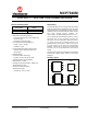
MCP7940M FIGURE 1-1: TYPICAL OPERATING CIRCUIT RTCC VCC Alarms and CLKOUT MFP Oscillator X1 X2 SCL NC I2C™ SRAM VSS SDA FIGURE 1-2: SCHEMATIC SYSTEM V CC C1 Note 1 R1 R2 R3 X1 V CC X2 MFP MFP SCL SCL SDA SDA CX1 CX2 NC V SS MCP7940M X1 Suggested Values: C1 100nF CX1, CX2 See Text R1 10K R2,3 2.2K X1 32.768 kHz Crystal (See Text) Note 1: A 100nF Capacitor should be placed as close to the VCC pin on the device as possible.
MCP7940M 1.0 ELECTRICAL CHARACTERISTICS Absolute Maximum Ratings (†) VCC.............................................................................................................................................................................6.5V All inputs and outputs w.r.t. VSS ..........................................................................................................-0.6V to VCC +1.0V Storage temperature .................................................................................
MCP7940M TABLE 1-2: AC CHARACTERISTICS Electrical Characteristics: Industrial (I): VCC = +1.8V to 5.5V AC CHARACTERISTICS Param. Symbol No. Characteristic Min. Max. Units TA = -40°C to +85°C Conditions 1 FCLK Clock frequency — — 100 400 kHz 1.8V VCC < 2.5V 2.5V VCC 5.5V 2 THIGH Clock high time 4000 600 — — ns 1.8V VCC < 2.5V 2.5V VCC 5.5V 3 TLOW Clock low time 4700 1300 — — ns 1.8V VCC < 2.5V 2.5V VCC 5.
MCP7940M FIGURE 1-3: BUS TIMING DATA 5 SCL 7 SDA In D4 2 3 8 9 4 10 6 13 11 12 SDA Out 2012 Microchip Technology Inc.
MCP7940M 2.0 PIN DESCRIPTIONS The descriptions of the pins are listed in Table 2-1. TABLE 2-1: PIN DESCRIPTIONS Pin Name VSS SDA SCL X1 X2 NC MFP VCC Pin Function Ground Bidirectional Serial Data Serial Clock Xtal Input, External Oscillator Input Xtal Output Not Connected Multi-Function Pin +1.8V to +5.5V Power Supply FIGURE 2-1: DEVICE PINOUTS SOIC/DFN/MSOP/TSSOP 2.
MCP7940M 3.0 I2C BUS CHARACTERISTICS 3.1.1.3 3.1 I2C Interface A low-to-high transition of the SDA line while the clock (SCL) is high determines a Stop condition. All operations must end with a Stop condition. The MCP7940M supports a bidirectional 2-wire bus and data transmission protocol. A device that sends data onto the bus is defined as transmitter, and a device receiving data as receiver.
MCP7940M FIGURE 3-2: ACKNOWLEDGE TIMING Acknowledge Bit 1 SCL 2 3 SDA 4 5 6 7 8 9 1 DEVICE ADDRESSING AND OPERATION A control byte is the first byte received following the Start condition from the master device (Figure 3-2). The control byte for accessing the SRAM and RTCC registers are set to ‘1101111’. The RTCC registers and the SRAM share the same address space. The last bit of the control byte defines the operation to be performed.
MCP7940M 4.0 RTCC FUNCTIONALITY FIGURE 4-1: The MCP7940M family is a highly integrated RTCC. On-board time and date counters are driven from a lowpower oscillator to maintain the time and date. 4.1 RTCC MEMORY MAP • Addresses 0x00h-0x06h are the RTCC Time and Date registers. These are read/write registers. Care must be taken when accessing these registers while the oscillator is running.
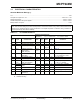
MCP7940M TABLE 4-1: Address 00h Bit 7 RTCC MEMORY MAP Bit 6 ST Bit 5 Bit 4 Bit 3 Bit 2 Bit 1 Bit 0 Function Range Reset State 10 Seconds Seconds Seconds 00-59 00h 01h 10 Minutes Minutes Minutes 00-59 00h 02h 10 Hour AM/PM Hours 1-12 + AM/PM 00 - 23 00h Day 1-7 01h Date 01-31 01h Month 01-12 01h Year 00-99 01h 12/24 Hour OSCON 03h 04h Day 10 Date 05h LP 06h 07h 10 Hour Date 10 Month Month 10 Year OUT SQWE Year ALM1 ALM0 EXTOSC RS2 08h CALIBRATION
MCP7940M 4.1.1 RTCC REGISTER ADDRESSES 0x00h – Contains the BCD seconds and 10 seconds. The range is 00 to 59. Bit 7 in this register is used to start or stop the on-board crystal oscillator. Setting this bit to a ‘1’ starts the oscillator and clearing this bit to a ‘0’ stops the on-board oscillator. 0x01h – Contains the BCD minutes and 10 minutes. The range is 00 to 59. 0x02h – Contains the BCD hour in bits 3:0.
MCP7940M 4.2 • ALMxC2:0: These Configuration bits determine the alarm match. The logic will trigger the alarm based on one of the following match conditions: FEATURES 4.2.1 000 – Seconds match 001 – Minutes match 010 – Hours match (takes into account 12/24 hour) 011 – Matches the current day, interrupt at 12.00.00 a.m. Example: 12 midnight on 100 – Date 101 – RESERVED 110 – RESERVED 111 – Seconds, Minutes, Hour, Day, Date, Month • The 12/24-hour bits 0xCh.6 and 0x13h.
MCP7940M With bits RS1 and RS0 set to ‘00’, the calibration function can be expressed as: = Toutput Since the calibration is done once per minute (i.e., when the internal minute counter is incremented), only one cycle in sixty of the MFP output waveform is affected by the calibration setting. Also note that the duty cycle of the MFP output waveform will not necessarily be at 50% when the calibration setting is applied.
MCP7940M 4.2.2 MFP Pin 7 is a multi-function pin and supports the following functions: • Use of the OUT bit in the Control register for single bit I/O • Alarm Outputs • FOUT mode – driven from a FOSC divider 4.2.3 CRYSTAL SPECS The MCP7940M has been designed to operate with a standard 32.768 kHz tuning fork crystal. The on-board oscillator has been characterized to operate with a crystal of maximum ESR of 70K Ohms. Crystals with a comparable specification are also suitable for use with the MCP7940M.
MCP7940M 5.0 ON BOARD MEMORY The MCP7940M has 64 x 8 bytes of on-chip SRAM. 5.
MCP7940M 5.2 5.2.1 RTCC/SRAM Pointer of the MCP7940M. After receiving another Acknowledge signal from the MCP7940M, the master device transmits the data word to be written into the addressed memory location. The MCP7940M acknowledges again and the master generates a Stop condition. After a Byte Write command, the internal address counter will point to the address location following the one that was just written.
MCP7940M 5.2.2.3 Sequential Read generate an Acknowledge but will generate a Stop condition. To provide sequential reads, the MCP7940M contains an internal Address Pointer which is incremented by one at the completion of each operation. This Address Pointer allows the entire memory contents to be serially read during one operation. The internal Address Pointer will automatically roll over to the start of the Block.
MCP7940M 6.0 PACKAGING INFORMATION 6.1 Package Marking Information 8-Lead PDIP Example: XXXXXXXX T/XXXNNN YYWW MCP7940M I/P e3 1L7 0528 Example: 8-Lead SOIC (3.90 mm) 7940MI SN e3 1133 13F XXXXXT XXYYWW NNN Example: 8-Lead TSSOP XXXX 940M TYWW I133 NNN 13F Example: 8-Lead MSOP XXXXX 7940MI YWWNNN 13313F 8-Lead 2x3 TDFN Example: XXX YWW NN AU1 133 13 Part Number MCP7940M Note: Legend: XX...
MCP7940M 3 & ' !& " & 4 # * !( ! ! & 4 % & & # & && 255*** ' '5 4 N NOTE 1 E1 1 3 2 D E A2 A L A1 c e eB b1 b 6 &! ' ! 9 ' &! 7"') % ! 7,8. 7 7 & ; < & & 7: 1 , = = - 1 ! & & = = .
MCP7940M Note: For the most current package drawings, please see the Microchip Packaging Specification located at http://www.microchip.com/packaging DS22292A-page 20 Preliminary 2012 Microchip Technology Inc.
MCP7940M Note: For the most current package drawings, please see the Microchip Packaging Specification located at http://www.microchip.com/packaging 2012 Microchip Technology Inc.
MCP7940M ! "" #$ %& ! ' 3 & ' !& " & 4 # * !( ! ! & 4 % & & # & && 255*** ' '5 4 DS22292A-page 22 Preliminary 2012 Microchip Technology Inc.
MCP7940M () )" * ! ( +%+ ( ! 3 & ' !& " & 4 # * !( ! ! & 4 % & & # & && 255*** ' '5 4 D N E E1 NOTE 1 1 2 b e c A φ A2 A1 L L1 6 &! ' ! 9 ' &! 7"') % ! 99 . . 7 7 7: ; < & : 8 & = = < = # # 4 4 !! & # %% ? 1 , : > #& . # # 4 > #& .
MCP7940M Note: For the most current package drawings, please see the Microchip Packaging Specification located at http://www.microchip.com/packaging DS22292A-page 24 Preliminary 2012 Microchip Technology Inc.
MCP7940M Note: For the most current package drawings, please see the Microchip Packaging Specification located at http://www.microchip.com/packaging 2012 Microchip Technology Inc.
MCP7940M Note: For the most current package drawings, please see the Microchip Packaging Specification located at http://www.microchip.com/packaging DS22292A-page 26 Preliminary 2012 Microchip Technology Inc.
MCP7940M Note: For the most current package drawings, please see the Microchip Packaging Specification located at http://www.microchip.com/packaging 2012 Microchip Technology Inc.
MCP7940M Note: For the most current package drawings, please see the Microchip Packaging Specification located at http://www.microchip.com/packaging DS22292A-page 28 Preliminary 2012 Microchip Technology Inc.
MCP7940M Note: For the most current package drawings, please see the Microchip Packaging Specification located at http://www.microchip.com/packaging 2012 Microchip Technology Inc.
MCP7940M , $ * - . /0 0 %12 ( , 3 & ' !& " & 4 # * !( ! ! & 4 % & & # & && 255*** ' '5 4 DS22292A-page 30 Preliminary 2012 Microchip Technology Inc.
MCP7940M APPENDIX A: REVISION HISTORY Revision A (02/2012) Original release of this document. 2012 Microchip Technology Inc.
MCP7940M NOTES: DS22292A-page 32 Preliminary 2012 Microchip Technology Inc.
MCP7940M THE MICROCHIP WEB SITE CUSTOMER SUPPORT Microchip provides online support via our WWW site at www.microchip.com. This web site is used as a means to make files and information easily available to customers.
MCP7940M READER RESPONSE It is our intention to provide you with the best documentation possible to ensure successful use of your Microchip product. If you wish to provide your comments on organization, clarity, subject matter, and ways in which our documentation can better serve you, please FAX your comments to the Technical Publications Manager at (480) 792-4150. Please list the following information, and use this outline to provide us with your comments about this document.
MCP7940M PRODUCT IDENTIFICATION SYSTEM To order or obtain information, e.g., on pricing or delivery, refer to the factory or the listed sales office. Not every possible ordering combination is listed below. PART NO. Device Device: X /XX Examples: Temperature Package Range MCP7940M = MCP7940MT= 1.8V - 5.5V I2C™ Serial RTCC 1.8V - 5.5V I2C Serial RTCC (Tape and Reel) Temperature Range: I = -40°C to +85°C Package: SN ST = = 8-Lead Plastic Small Outline (3.
MCP7940M NOTES: DS22292A-page 36 Preliminary 2012 Microchip Technology Inc.
Note the following details of the code protection feature on Microchip devices: • Microchip products meet the specification contained in their particular Microchip Data Sheet. • Microchip believes that its family of products is one of the most secure families of its kind on the market today, when used in the intended manner and under normal conditions. • There are dishonest and possibly illegal methods used to breach the code protection feature.
Worldwide Sales and Service AMERICAS ASIA/PACIFIC ASIA/PACIFIC EUROPE Corporate Office 2355 West Chandler Blvd. Chandler, AZ 85224-6199 Tel: 480-792-7200 Fax: 480-792-7277 Technical Support: http://www.microchip.com/ support Web Address: www.microchip.