
Datasheet


© 2009 Microchip Technology Inc. DS22005B-page 3
MCP73833/4
1.0 ELECTRICAL
CHARACTERISTICS
Absolute Maximum Ratings
V
DD
........................................................................7.0V
All Inputs and Outputs w.r.t. V
SS
.....-0.3 to (V
DD
+0.3)V
Maximum Junction Temperature, T
J
. Internally Limited
Storage temperature ..........................-65°C to +150°C
ESD protection on all pins:
Human Body Model (HBM)
(1.5 kΩ in Series with 100 pF)............................... ≥ 4kV
Machine Model (MM)
(200 pF, No Series Resistance) ...........................300V
*Notice: Stresses above those listed under “Maximum
Ratings” may cause permanent damage to the device.
This is a stress rating only and functional operation of
the device at those or any other conditions above those
indicated in the operational listings of this specification
is not implied. Exposure to maximum rating conditions
for extended periods may affect device reliability.
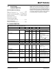
DC CHARACTERISTICS
Electrical Specifications: Unless otherwise specified, all limits apply for V
DD
= [V
REG
(Typical)+0.3V] to 6V, T
A
=-40°C to 85°C.
Typical values are at +25°C, V
DD
= [V
REG
(Typical)+1.0V]
Parameters Sym Min Typ Max Units Conditions
Supply Input
Supply Voltage V
DD
3.75 — 6 V Charging
V
REG
(Typ-
ical)+0.3V
— 6 V Charge Complete, Standby
Supply Current I
SS
— 2000 3000 µA Charging
— 150 300 µA Charge Complete
— 100 300 µA Standby (No Battery or PROG
Floating)
— 50 100 µA Shutdown (V
DD
< V
BAT
, or
V
DD
< V
STOP
)
UVLO Start Threshold V
START
3.4 3.55 3.7 V V
DD
Low-to-High
UVLO Stop Threshold V
STOP
3.3 3.45 3.6 V V
DD
High-to-Low
UVLO Hysteresis V
HYS
— 100 — mV
Voltage Regulation (Constant Voltage Mode, System Test Mode)
Regulated Output Voltage V
REG
4.168 4.20 4.232 V V
DD
=[V
REG
(Typical)+1V]
4.318 4.35 4.382 V I
OUT
=10 mA
4.367 4.40 4.433 V T
A
=-5°C to +55°C
4.467 4.50 4.533 V
Line Regulation |(ΔV
BAT
/V
BAT
)
/ΔV
DD
|
— 0.10 0.30 %/V V
DD
=[V
REG
(Typical)+1V] to
6V, I
OUT
=10 mA
Load Regulation |ΔV
BAT
/ V
BAT
| — 0.10 0.30 % I
OUT
=10 mA to 100 mA
V
DD
=[V
REG
(Typical)+1V]
Supply Ripple Attenuation PSRR — 58 — dB I
OUT
=10 mA, 10Hz to 1 kHz
—47— dBI
OUT
=10 mA, 10Hz to 10 kHz
—25— dBI
OUT
=10 mA, 10Hz to 1 MHz
Current Regulation (Fast Charge Constant Current Mode)
Fast Charge Current Regulation I
REG
90 100 110 mA PROG = 10 kΩ
900 1000 1100 mA PROG = 1.0 kΩ
T
A
=-5°C to +55°C
Maximum Output Current Limit I
MAX
— 1200 — mA PROG < 833Ω